ZHCSUH0G August   2007  – January 2024 CDCE949 , CDCEL949

PRODUCTION DATA  

  1.   1
  2. 特性
  3. 应用
  4. 说明
  5. Pin Configuration and Functions
  6. Specifications
    1. 5.1 Absolute Maximum Ratings
    2. 5.2 ESD Ratings
    3. 5.3 Recommended Operating Conditions
    4. 5.4 Thermal Information
    5. 5.5 Electrical Characteristics
    6. 5.6 EEPROM Specification
    7. 5.7 Timing Requirements: CLK_IN
    8. 5.8 Timing Requirements: SDA/SCL
    9. 5.9 Typical Characteristics
  7. Parameter Measurement Information
  8. Detailed Description
    1. 7.1 Overview
    2. 7.2 Functional Block Diagram
    3. 7.3 Feature Description
      1. 7.3.1 Control Terminal Setting
      2. 7.3.2 Default Device Setting
      3. 7.3.3 SDA/SCL Serial Interface
      4. 7.3.4 Data Protocol
    4. 7.4 Device Functional Modes
      1. 7.4.1 SDA/SCL Hardware Interface
    5. 7.5 Programming
  9. Application and Implementation
    1. 8.1 Application Information
    2. 8.2 Typical Application
      1. 8.2.1 Design Requirements
      2. 8.2.2 Detailed Design Procedure
        1. 8.2.2.1 Spread Spectrum Clock (SSC)
        2. 8.2.2.2 PLL Frequency Planning
        3. 8.2.2.3 Crystal Oscillator Start-Up
        4. 8.2.2.4 Frequency Adjustment With Crystal Oscillator Pulling
        5. 8.2.2.5 Unused Inputs and Outputs
        6. 8.2.2.6 Switching Between XO and VCXO Mode
      3. 8.2.3 Application Curves
    3. 8.3 Power Supply Recommendations
    4. 8.4 Layout
      1. 8.4.1 Layout Guidelines
      2. 8.4.2 Layout Example
  10. Register Maps
    1. 9.1 SDA/SCL Configuration Registers
  11. 10Device and Documentation Support
    1. 10.1 Device Support
      1. 10.1.1 Development Support
    2. 10.2 Related Documentation
    3. 10.3 Related Links
    4. 10.4 接收文档更新通知
    5. 10.5 支持资源
    6. 10.6 Trademarks
    7. 10.7 静电放电警告
    8. 10.8 术语表
  12. 11Revision History
  13. 12Mechanical, Packaging, and Orderable Information

封装选项

机械数据 (封装 | 引脚)
散热焊盘机械数据 (封装 | 引脚)
订购信息

Programming

Table 7-6 Command Code Definition
BITDESCRIPTION
70 = Block Read or Block Write operation
1 = Byte Read or Byte Write operation
(6:0)Byte Offset for Byte Read, Block Read, Byte Write and Block Write operation.
Figure 7-4 Generic Programming SequenceGUID-1C6526CF-C7F5-401C-8667-B005BE4C6C82-low.gif

GUID-20231108-SS0I-BD30-X45R-D0VX1JTJSBXW-low.gif
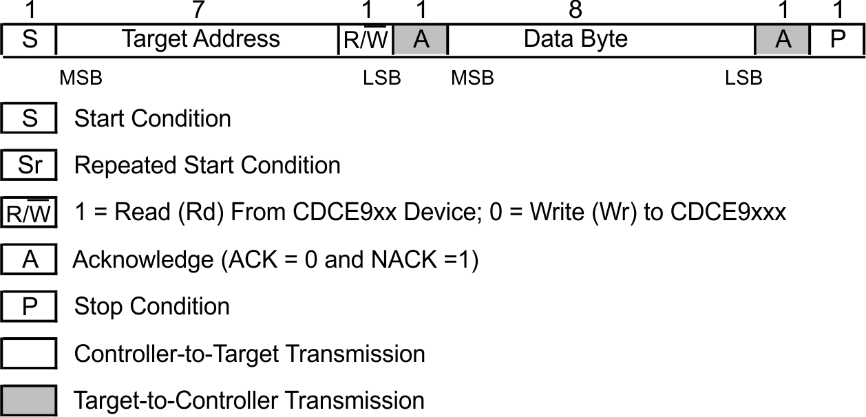
Figure 7-5 Byte Write Protocol
GUID-34ED2741-320B-48A4-A5CB-E817069994D7-low.svg Figure 7-6 Byte Read Protocol

GUID-20231108-SS0I-NHBN-WWMW-T9MJBHLZ9GLH-low.gif
Data Byte 0 Bits [7:0] are reserved for Revision Code and Vendor Identification. The Data Byte 0 is used for internal test purpose and must not be overwritten.
Figure 7-7 Block Write Programming
GUID-C8807933-3163-4A32-9369-9495D50A1025-low.gif Figure 7-8 Block Read Protocol
GUID-F1BB3137-BD3D-43D6-A6CA-DCD56AA44022-low.gifFigure 7-9 Timing Diagram for the SDA/SCL Serial Control Interface