ZHCSUH0G August 2007 – January 2024 CDCE949 , CDCEL949
PRODUCTION DATA
- 1
- 1 特性
- 2 应用
- 3 说明
- 4 Pin Configuration and Functions
- 5 Specifications
- 6 Parameter Measurement Information
- 7 Detailed Description
- 8 Application and Implementation
- 9 Register Maps
- 10Device and Documentation Support
- 11Revision History
- 12Mechanical, Packaging, and Orderable Information
9.1 SDA/SCL Configuration Registers
The clock input, control pins, PLLs, and output stages are user configurable. The following tables and explanations describe the programmable functions of the CDCEx949. All settings can be manually written to the device through the SDA/SCL bus, or are easily programmable by using the TI Pro Clock software. TI Pro Clock software allows the user to quickly make all settings and automatically calculates the values for optimized performance at lowest jitter.
| ADDRESS OFFSET | REGISTER DESCRIPTION | TABLE |
|---|---|---|
| 00h | Generic configuration register | Table 9-3 |
| 10h | PLL1 configuration register | Table 9-4 |
| 20h | PLL2 configuration register | Table 9-5 |
| 30h | PLL3 configuration register | Table 9-6 |
| 40h | PLL4 configuration register | Table 9-7 |
The grey-highlighted Bits described in the configuration registers tables on the following pages, belong to the Control Pin Register. The user can predefine up to eight different control settings. These settings can then be selected by the external control pins, S0, S1, and S2 (see Control Terminal Setting).
| EXTERNAL CONTROL PINS | Y1 | PLL1 SETTING | PLL2 SETTING | PLL3 SETTING | PLL4 SETTING | ||||||||||
|---|---|---|---|---|---|---|---|---|---|---|---|---|---|---|---|
| OUTPUT SELECT | FREQ SELECT | SSC SELECT | OUTPUT SELECT | FREQ SELECT | SSC SELECT | OUTPUT SELECT | FREQ SELECT | SSC SELECT | OUTPUT SELECT | FREQ SELECT | SSC SELECT | OUTPUT SELECT | |||
| S2 | S1 | S0 | Y1 | FS1 | SSC1 | Y2Y3 | FS2 | SSC2 | Y4Y5 | FS3 | SSC3 | Y6Y7 | FS4 | SSC4 | Y8Y9 |
| 0 | 0 | 0 | Y1_0 | FS1_0 | SSC1_0 | Y2Y3_0 | FS2_0 | SSC2_0 | Y4Y5_0 | FS3_0 | SSC3_0 | Y6Y7_0 | FS4_0 | SSC4_0 | Y8Y9_0 |
| 0 | 0 | 1 | Y1_1 | FS1_1 | SSC1_1 | Y2Y3_1 | FS2_1 | SSC2_1 | Y4Y5_1 | FS3_1 | SSC3_1 | Y6Y7_1 | FS4_1 | SSC4_1 | Y8Y9_1 |
| 0 | 1 | 0 | Y1_2 | FS1_2 | SSC1_2 | Y2Y3_2 | FS2_2 | SSC2_2 | Y4Y5_2 | FS3_2 | SSC3_2 | Y6Y7_2 | FS4_2 | SSC4_2 | Y8Y9_2 |
| 0 | 1 | 1 | Y1_3 | FS1_3 | SSC1_3 | Y2Y3_3 | FS2_3 | SSC2_3 | Y4Y5_3 | FS3_3 | SSC3_3 | Y6Y7_3 | FS4_3 | SSC4_3 | Y8Y9_3 |
| 1 | 0 | 0 | Y1_4 | FS1_4 | SSC1_4 | Y2Y3_4 | FS2_4 | SSC2_4 | Y4Y5_4 | FS3_4 | SSC3_4 | Y6Y7_4 | FS4_4 | SSC4_4 | Y8Y9_4 |
| 1 | 0 | 1 | Y1_5 | FS1_5 | SSC1_5 | Y2Y3_5 | FS2_5 | SSC2_5 | Y4Y5_5 | FS3_5 | SSC3_5 | Y6Y7_5 | FS4_5 | SSC4_5 | Y8Y9_5 |
| 1 | 1 | 0 | Y1_6 | FS1_6 | SSC1_6 | Y2Y3_6 | FS2_6 | SSC2_6 | Y4Y5_6 | FS3_6 | SSC3_6 | Y6Y7_6 | FS4_6 | SSC4_6 | Y8Y9_6 |
| 1 | 1 | 1 | Y1_7 | FS1_7 | SSC1_7 | Y2Y3_7 | FS2_7 | SSC2_7 | Y4Y5_7 | FS3_7 | SSC3_7 | Y6Y7_7 | FS4_7 | SSC4_7 | Y8Y9_7 |
| Addr. Offset(1) | 04h | 13h | 10h-12h | 15h | 23h | 20h-22h | 25h | 33h | 30h-32h | 35h | 43h | 40h-42h | 45h | ||
| OFFSET(1) | BIT(2) | ACRONYM | DEFAULT(3) | DESCRIPTION | |||
|---|---|---|---|---|---|---|---|
| 00h | 7 | E_EL | xb | Device Identification (read only): ‘1’ is CDCE949 (3.3V), ‘0’ is CDCEL949 (1.8V) | |||
| 6:4 | RID | Xb | Revision Identification Number (read only) | ||||
| 3:0 | VID | 1h | Vendor Identification Number (read only) | ||||
| 01h | 7 | – | 0b | Reserved - always write 0 | |||
| 6 | EEPIP | 0b | EEPROM Programming Status(4): (read only) | 0 – EEPROM programming is completed 1 – EEPROM is in programming mode | |||
| 5 | EELOCK | 0b | Permanently Lock EEPROM Data(5): | 0 – EEPROM is not locked 1 – EEPROM is permanently locked | |||
| 4 | PWDN | 0b | Device power down (overwrites S0/S1/S2 setting; configuration register settings are unchanged) Note: PWDN cannot be set to 1 in the EEPROM. | ||||
| 0 – device active (all PLLs and all outputs are enabled) 1 – device power down (all PLLs in power down and all outputs in 3-State) | |||||||
| 3:2 | INCLK | 00b | Input clock selection: | 00 – X-tal 01 – VCXO | 10 – LVCMOS 11 – reserved | ||
| 1:0 | TARGET_ADR | 00b | Programmable Address Bits A0 and A1 of the Target Receiver Address | ||||
| 02h | 7 | M1 | 1b | Clock source selection for output Y1: | 0 – input clock 1 – PLL1 clock | ||
| 6 | SPICON | 0b | Operation mode selection for pin 22/23(6) | ||||
| 0 – serial programming interface SDA (pin 23) and SCL (pin 22) 1 – control pins S1 (pin 23) and S2 (pin 22) | |||||||
| 5:4 | Y1_ST1 | 11b | Y1-State0/1 Definition (applies to Y1_ST1 and Y1_ST0) | ||||
| 3:2 | Y1_ST0 | 01b | 00 – device power down (all PLLs in power down and all outputs in 3-state) 01 – Y1 disabled to 3-state 10 – Y1 disabled to low 11 – Y1 enabled (normal operation) | ||||
| 1:0 | Pdiv1 [9:8] | 001h | 10-Bit Y1-Output-Divider Pdiv1: | 0 – divider reset and stand-by 1-to-1023 – divider value | |||
| 03h | 7:0 | Pdiv1 [7:0] | |||||
| 04h | 7 | Y1_7 | 0b | Y1_x State Selection(7) | |||
| 6 | Y1_6 | 0b | 0 – State0 (predefined by Y1-State0 Definition [Y1_ST0]) 1 – State1 (predefined by Y1-State1 Definition [Y1_ST1]) | ||||
| 5 | Y1_5 | 0b | |||||
| 4 | Y1_4 | 0b | |||||
| 3 | Y1_3 | 0b | |||||
| 2 | Y1_2 | 0b | |||||
| 1 | Y1_1 | 1b | |||||
| 0 | Y1_0 | 0b | |||||
| 05h | 7:3 | XCSEL | 0Ah | Crystal load capacitor selection(8): | 00h → 0 pF 01h → 1 pF 02h → 2 pF 14h-to-1Fh → 20 pF | 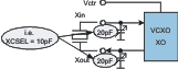 | |
| 2:0 | — | 0b | Reserved - do not write others than 0 | ||||
| 06h | 7:1 | BCOUNT | 50h | 7-Bit Byte Count (Defines the number of Bytes which is sent from this device at the next Block Read transfer; all bytes must be read out to correctly finish the read cycle.) | |||
| 0 | EEWRITE | 0b | Initiate EEPROM Write Cycle(4)(9) | ||||
| 0 – no EEPROM write cycle 1 – start EEPROM write cycle (internal configuration register is saved to the EEPROM) | |||||||
| 07h-0Fh | — | — | 0h | Reserved – do not write others than 0 | |||
| OFFSET(1) | BIT(2) | ACRONYM | DEFAULT(3) | DESCRIPTION | |||
|---|---|---|---|---|---|---|---|
| 10h | 7:5 | SSC1_7 [2:0] | 000b | SSC1: PLL1 SSC Selection (Modulation Amount)(4) | |||
| 4:2 | SSC1_6 [2:0] | 000b | Down 000 (off) 001 – 0.25% 010 – 0.5% 011 – 0.75% 100 – 1.0% 101 – 1.25% 110 – 1.5% 111 – 2.0% | Center 000 (off) 001 ± 0.25% 010 ± 0.5% 011 ± 0.75% 100 ± 1.0% 101 ± 1.25% 110 ± 1.5% 111 ± 2.0% | |||
| 1:0 | SSC1_5 [2:1] | 000b | |||||
| 11h | 7 | SSC1_5 [0] | |||||
| 6:4 | SSC1_4 [2:0] | 000b | |||||
| 3:1 | SSC1_3 [2:0] | 000b | |||||
| 0 | SSC1_2 [2] | 000b | |||||
| 12h | 7:6 | SSC1_2 [1:0] | |||||
| 5:3 | SSC1_1 [2:0] | 000b | |||||
| 2:0 | SSC1_0 [2:0] | 000b | |||||
| 13h | 7 | FS1_7 | 0b | FS1_x: PLL1 Frequency Selection(4) | |||
| 6 | FS1_6 | 0b | 0 – fVCO1_0 (predefined by PLL1_0 – Multiplier/Divider value) 1 – fVCO1_1 (predefined by PLL1_1 – Multiplier/Divider value) | ||||
| 5 | FS1_5 | 0b | |||||
| 4 | FS1_4 | 0b | |||||
| 3 | FS1_3 | 0b | |||||
| 2 | FS1_2 | 0b | |||||
| 1 | FS1_1 | 0b | |||||
| 0 | FS1_0 | 0b | |||||
| 14h | 7 | MUX1 | 1b | PLL1 Multiplexer: | 0 – PLL1 1 – PLL1 Bypass (PLL1 is in power down) | ||
| 6 | M2 | 1b | Output Y2 Multiplexer: | 0 – Pdiv1 1 – Pdiv2 | |||
| 5:4 | M3 | 10b | Output Y3 Multiplexer: | 00 – Pdiv1-Divider 01 – Pdiv2-Divider 10 – Pdiv3-Divider 11 – reserved | |||
| 3:2 | Y2Y3_ST1 | 11b | Y2, Y3-State0/1definition: | 00 – Y2/Y3 disabled to 3-State (PLL1 is in power down) 01 – Y2/Y3 disabled to 3-State (PLL1 on) 10–Y2/Y3 disabled to low (PLL1 on) 11 – Y2/Y3 enabled (normal operation, PLL1 on) | |||
| 1:0 | Y2Y3_ST0 | 01b | |||||
| 15h | 7 | Y2Y3_7 | 0b | Y2Y3_x Output State Selection(4) | |||
| 6 | Y2Y3_6 | 0b | 0 – state0 (predefined by Y2Y3_ST0) 1 – state1 (predefined by Y2Y3_ST1) | ||||
| 5 | Y2Y3_5 | 0b | |||||
| 4 | Y2Y3_4 | 0b | |||||
| 3 | Y2Y3_3 | 0b | |||||
| 2 | Y2Y3_2 | 0b | |||||
| 1 | Y2Y3_1 | 1b | |||||
| 0 | Y2Y3_0 | 0b | |||||
| 16h | 7 | SSC1DC | 0b | PLL1 SSC down/center selection: | 0 – down 1 – center | ||
| 6:0 | Pdiv2 | 01h | 7-Bit Y2-Output-Divider Pdiv2: | 0 – reset and stand-by 1-to-127 – divider value | |||
| 17h | 7 | — | 0b | Reserved – do not write others than 0 | |||
| 6:0 | Pdiv3 | 01h | 7-Bit Y3-Output-Divider Pdiv3: | 0 – reset and stand-by 1-to-127 – divider value | |||
| 18h | 7:0 | PLL1_0N [11:4 | 004h | PLL1_0(5): 30-Bit Multiplier/Divider value for frequency fVCO1_0 (for more information, see PLL Frequency Planning) | |||
| 19h | 7:4 | PLL1_0N [3:0] | |||||
| 3:0 | PLL1_0R [8:5] | 000h | |||||
| 1Ah | 7:3 | PLL1_0R[4:0] | |||||
| 2:0 | PLL1_0Q [5:3] | 10h | |||||
| 1Bh | 7:5 | PLL1_0Q [2:0] | |||||
| 4:2 | PLL1_0P [2:0] | 010b | |||||
| 1:0 | VCO1_0_RANGE | 00b | fVCO1_0 range selection: | 00 – fVCO1_0 < 125 MHz 01 – 125 MHz ≤ fVCO1_0 < 150 MHz 10 – 150 MHz ≤ fVCO1_0 < 175 MHz 11 – fVCO1_0 ≥ 175 MHz | |||
| 1Ch | 7:0 | PLL1_1N [11:4] | 004h | PLL1_1(5): 30-Bit Multiplier/Divider value for frequency fVCO1_1 (for more information, see PLL Frequency Planning). | |||
| 1Dh | 7:4 | PLL1_1N [3:0] | |||||
| 3:0 | PLL1_1R [8:5] | 000h | |||||
| 1Eh | 7:3 | PLL1_1R[4:0] | |||||
| 2:0 | PLL1_1Q [5:3] | 10h | |||||
| 1Fh | 7:5 | PLL1_1Q [2:0] | |||||
| 4:2 | PLL1_1P [2:0] | 010b | |||||
| 1:0 | VCO1_1_RANGE | 00b | fVCO1_1 range selection: | 00 – fVCO1_1 < 125 MHz 01 – 125 MHz ≤ fVCO1_1 < 150 MHz 10 – 150 MHz ≤ fVCO1_1 < 175 MHz 11 – fVCO1_1 ≥ 175 MHz | |||
| OFFSET(1) | BIT(2) | ACRONYM | DEFAULT(3) | DESCRIPTION | |||
|---|---|---|---|---|---|---|---|
| 20h | 7:5 | SSC2_7 [2:0] | 000b | SSC2: PLL2 SSC Selection (Modulation Amount)(4) | |||
| 4:2 | SSC2_6 [2:0] | 000b | Down 000 (off) 001 – 0.25% 010 – 0.5% 011 – 0.75% 100 – 1.0% 101 – 1.25% 110 – 1.5% 111 – 2.0% | Center 000 (off) 001 ± 0.25% 010 ± 0.5% 011 ± 0.75% 100 ± 1.0% 101 ± 1.25% 110 ± 1.5% 111 ± 2.0% | |||
| 1:0 | SSC2_5 [2:1] | 000b | |||||
| 21h | 7 | SSC2_5 [0] | |||||
| 6:4 | SSC2_4 [2:0] | 000b | |||||
| 3:1 | SSC2_3 [2:0] | 000b | |||||
| 0 | SSC2_2 [2] | 000b | |||||
| 22h | 7:6 | SSC2_2 [1:0] | |||||
| 5:3 | SSC2_1 [2:0] | 000b | |||||
| 2:0 | SSC2_0 [2:0] | 000b | |||||
| 23h | 7 | FS2_7 | 0b | FS2_x: PLL2 Frequency Selection(4) | |||
| 6 | FS2_6 | 0b | 0 – fVCO2_0 (predefined by PLL2_0 – Multiplier/Divider value) 1 – fVCO2_1 (predefined by PLL2_1 – Multiplier/Divider value) | ||||
| 5 | FS2_5 | 0b | |||||
| 4 | FS2_4 | 0b | |||||
| 3 | FS2_3 | 0b | |||||
| 2 | FS2_2 | 0b | |||||
| 1 | FS2_1 | 0b | |||||
| 0 | FS2_0 | 0b | |||||
| 24h | 7 | MUX2 | 1b | PLL2 Multiplexer: | 0 – PLL2 1 – PLL2 Bypass (PLL2 is in power down) | ||
| 6 | M4 | 1b | Output Y4 Multiplexer: | 0 – Pdiv2 1 – Pdiv4 | |||
| 5:4 | M5 | 10b | Output Y5 Multiplexer: | 00 – Pdiv2-Divider 01 – Pdiv4-Divider 10 – Pdiv5-Divider 11 – reserved | |||
| 3:2 | Y4Y5_ST1 | 11b | Y4, Y5-State0/1definition: | 00 – Y4/Y5 disabled to 3-State (PLL2 is in power down) 01 – Y4/Y5 disabled to 3-State (PLL2 on) 10–Y4/Y5 disabled to low (PLL2 on) 11 – Y4/Y5 enabled (normal operation, PLL2 on) | |||
| 1:0 | Y4Y5_ST0 | 01b | |||||
| 25h | 7 | Y4Y5_7 | 0b | Y4Y5_x Output State Selection(4) | |||
| 6 | Y4Y5_6 | 0b | 0 – state0 (predefined by Y4Y5_ST0) 1 – state1 (predefined by Y4Y5_ST1) | ||||
| 5 | Y4Y5_5 | 0b | |||||
| 4 | Y4Y5_4 | 0b | |||||
| 3 | Y4Y5_3 | 0b | |||||
| 2 | Y4Y5_2 | 0b | |||||
| 1 | Y4Y5_1 | 1b | |||||
| 0 | Y4Y5_0 | 0b | |||||
| 26h | 7 | SSC2DC | 0b | PLL2 SSC down/center selection: | 0 – down 1 – center | ||
| 6:0 | Pdiv4 | 01h | 7-Bit Y4-Output-Divider Pdiv4: | 0 – reset and stand-by 1-to-127 – divider value | |||
| 27h | 7 | — | 0b | Reserved – do not write others than 0 | |||
| 6:0 | Pdiv5 | 01h | 7-Bit Y5-Output-Divider Pdiv5: | 0 – reset and stand-by 1-to-127 – divider value | |||
| 28h | 7:0 | PLL2_0N [11:4 | 004h | PLL2_0(5): 30-Bit Multiplier/Divider value for frequency fVCO2_0 (for more information, see PLL Frequency Planning). | |||
| 29h | 7:4 | PLL2_0N [3:0] | |||||
| 3:0 | PLL2_0R [8:5] | 000h | |||||
| 2Ah | 7:3 | PLL2_0R[4:0] | |||||
| 2:0 | PLL2_0Q [5:3] | 10h | |||||
| 2Bh | 7:5 | PLL2_0Q [2:0] | |||||
| 4:2 | PLL2_0P [2:0] | 010b | |||||
| 1:0 | VCO2_0_RANGE | 00b | fVCO2_0 range selection: | 00 – fVCO2_0 < 125 MHz 01 – 125 MHz ≤ fVCO2_0 < 150 MHz 10 – 150 MHz ≤ fVCO2_0 < 175 MHz 11 – fVCO2_0 ≥ 175 MHz | |||
| 2Ch | 7:0 | PLL2_1N [11:4] | 004h | PLL2_1(5): 30-Bit Multiplier/Divider value for frequency fVCO1_1 (for more information, see PLL Frequency Planning). | |||
| 2Dh | 7:4 | PLL2_1N [3:0] | |||||
| 3:0 | PLL2_1R [8:5] | 000h | |||||
| 2Eh | 7:3 | PLL2_1R[4:0] | |||||
| 2:0 | PLL2_1Q [5:3] | 10h | |||||
| 2Fh | 7:5 | PLL2_1Q [2:0] | |||||
| 4:2 | PLL2_1P [2:0] | 010b | |||||
| 1:0 | VCO2_1_RANGE | 00b | fVCO2_1 range selection: | 00 – fVCO2_1 < 125 MHz 01 – 125 MHz ≤ fVCO2_1 < 150 MHz 10 – 150 MHz ≤ fVCO2_1 < 175 MHz 11 – fVCO2_1 ≥ 175 MHz | |||
| OFFSET(1) | BIT(2) | ACRONYM | DEFAULT(3) | DESCRIPTION | |||
|---|---|---|---|---|---|---|---|
| 30h | 7:5 | SSC3_7 [2:0] | 000b | SSC3: PLL3 SSC Selection (Modulation Amount)(4) | |||
| 4:2 | SSC3_6 [2:0] | 000b | Down 000 (off) 001 – 0.25% 010 – 0.5% 011 – 0.75% 100 – 1.0% 101 – 1.25% 110 – 1.5% 111 – 2.0% | Center 000 (off) 001 ± 0.25% 010 ± 0.5% 011 ± 0.75% 100 ± 1.0% 101 ± 1.25% 110 ± 1.5% 111 ± 2.0% | |||
| 1:0 | SSC3_5 [2:1] | 000b | |||||
| 31h | 7 | SSC3_5 [0] | |||||
| 6:4 | SSC3_4 [2:0] | 000b | |||||
| 3:1 | SSC3_3 [2:0] | 000b | |||||
| 0 | SSC3_2 [2] | 000b | |||||
| 32h | 7:6 | SSC3_2 [1:0] | |||||
| 5:3 | SSC3_1 [2:0] | 000b | |||||
| 2:0 | SSC3_0 [2:0] | 000b | |||||
| 33h | 7 | FS3_7 | 0b | FS3_x: PLL3 Frequency Selection(4) | |||
| 6 | FS3_6 | 0b | 0 – fVCO3_0 (predefined by PLL3_0 – Multiplier/Divider value) 1 – fVCO3_1 (predefined by PLL3_1 – Multiplier/Divider value) | ||||
| 5 | FS3_5 | 0b | |||||
| 4 | FS3_4 | 0b | |||||
| 3 | FS3_3 | 0b | |||||
| 2 | FS3_2 | 0b | |||||
| 1 | FS3_1 | 0b | |||||
| 0 | FS3_0 | 0b | |||||
| 34h | 7 | MUX3 | 1b | PLL3 Multiplexer: | 0 – PLL3 1 – PLL3 Bypass (PLL3 is in power down) | ||
| 6 | M6 | 1b | Output Y6 Multiplexer: | 0 – Pdiv4 1 – Pdiv6 | |||
| 5:4 | M7 | 10b | Output Y7 Multiplexer: | 00 – Pdiv4-Divider 01 – Pdiv6-Divider 10 – Pdiv7-Divider 11 – reserved | |||
| 3:2 | Y6Y7_ST1 | 11b | Y6, Y7-State0/1definition: | 00 – Y6/Y7 disabled to 3-State (PLL3 is in power down) 01 – Y6/Y7 disabled to 3-State (PLL3 on) 10 –Y6/Y7 disabled to low (PLL3 on) 11 – Y6/Y7 enabled (normal operation, PLL3 on) | |||
| 1:0 | Y6Y7_ST0 | 01b | |||||
| 35h | 7 | Y6Y7_7 | 0b | Y6Y7_x Output State Selection(4) | |||
| 6 | Y6Y7_6 | 0b | 0 – state0 (predefined by Y6Y7_ST0) 1 – state1 (predefined by Y6Y7_ST1) | ||||
| 5 | Y6Y7_5 | 0b | |||||
| 4 | Y6Y7_4 | 0b | |||||
| 3 | Y6Y7_3 | 0b | |||||
| 2 | Y6Y7_2 | 0b | |||||
| 1 | Y6Y7_1 | 1b | |||||
| 0 | Y6Y7_0 | 0b | |||||
| 36h | 7 | SSC3DC | 0b | PLL3 SSC down/center selection: | 0 – down 1 – center | ||
| 6:0 | Pdiv6 | 01h | 7-Bit Y6-Output-Divider Pdiv6: | 0 – reset and stand-by 1-to-127 – divider value | |||
| 37h | 7 | — | 0b | Reserved – do not write others than 0 | |||
| 6:0 | Pdiv7 | 01h | 7-Bit Y7-Output-Divider Pdiv7: | 0 – reset and stand-by 1-to-127 – divider value | |||
| 38h | 7:0 | PLL3_0N [11:4 | 004h | PLL3_0(5): 30-Bit Multiplier/Divider value for frequency fVCO3_0 (for more information, see PLL Frequency Planning). | |||
| 39h | 7:4 | PLL3_0N [3:0] | |||||
| 3:0 | PLL3_0R [8:5] | 000h | |||||
| 3Ah | 7:3 | PLL3_0R[4:0] | |||||
| 2:0 | PLL3_0Q [5:3] | 10h | |||||
| 3Bh | 7:5 | PLL3_0Q [2:0] | |||||
| 4:2 | PLL3_0P [2:0] | 010b | |||||
| 1:0 | VCO3_0_RANGE | 00b | fVCO3_0 range selection: | 00 – fVCO3_0 < 125 MHz 01 – 125 MHz ≤ fVCO3_0 < 150 MHz 10 – 150 MHz ≤ fVCO3_0 < 175 MHz 11 – fVCO3_0 ≥ 175 MHz | |||
| 3Ch | 7:0 | PLL3_1N [11:4] | 004h | PLL3_1(5): 30-Bit Multiplier/Divider value for frequency fVCO3_1 (for more information, see PLL Frequency Planning). | |||
| 3Dh | 7:4 | PLL3_1N [3:0] | |||||
| 3:0 | PLL3_1R [8:5] | 000h | |||||
| 3Eh | 7:3 | PLL3_1R[4:0] | |||||
| 2:0 | PLL3_1Q [5:3] | 10h | |||||
| 3Fh | 7:5 | PLL3_1Q [2:0] | |||||
| 4:2 | PLL3_1P [2:0] | 010b | |||||
| 1:0 | VCO3_1_RANGE | 00b | fVCO3_1 range selection: | 00 – fVCO3_1 < 125 MHz 01 – 125 MHz ≤ fVCO3_1 < 150 MHz 10 – 150 MHz ≤ fVCO3_1 < 175 MHz 11 – fVCO3_1 ≥ 175 MHz | |||
| OFFSET(1) | BIT(2) | ACRONYM | DEFAULT(3) | DESCRIPTION | |||
|---|---|---|---|---|---|---|---|
| 40h | 7:5 | SSC4_7 [2:0] | 000b | SSC4: PLL4 SSC Selection (Modulation Amount)(4) | |||
| 4:2 | SSC4_6 [2:0] | 000b | Down 000 (off) 001 – 0.25% 010 – 0.5% 011 – 0.75% 100 – 1.0% 101 – 1.25% 110 – 1.5% 111 – 2.0% | Center 000 (off) 001 ± 0.25% 010 ± 0.5% 011 ± 0.75% 100 ± 1.0% 101 ± 1.25% 110 ± 1.5% 111 ± 2.0% | |||
| 1:0 | SSC4_5 [2:1] | 000b | |||||
| 41h | 7 | SSC4_5 [0] | |||||
| 6:4 | SSC4_4 [2:0] | 000b | |||||
| 3:1 | SSC4_3 [2:0] | 000b | |||||
| 0 | SSC4_2 [2] | 000b | |||||
| 42h | 7:6 | SSC4_2 [1:0] | |||||
| 5:3 | SSC4_1 [2:0] | 000b | |||||
| 2:0 | SSC4_0 [2:0] | 000b | |||||
| 43h | 7 | FS4_7 | 0b | FS4_x: PLL4 Frequency Selection(4)sl | |||
| 6 | FS4_6 | 0b | 0 – fVCO4_0 (predefined by PLL4_0 – Multiplier/Divider value) 1 – fVCO4_1 (predefined by PLL4_1 – Multiplier/Divider value) | ||||
| 5 | FS4_5 | 0b | |||||
| 4 | FS4_4 | 0b | |||||
| 3 | FS4_3 | 0b | |||||
| 2 | FS4_2 | 0b | |||||
| 1 | FS4_1 | 0b | |||||
| 0 | FS4_0 | 0b | |||||
| 44h | 7 | MUX4 | 1b | PLL4 Multiplexer: | 0 – PLL4 1 – PLL4 Bypass (PLL4 is in power down) | ||
| 6 | M8 | 1b | Output Y8 Multiplexer: | 0 – Pdiv6 1 – Pdiv8 | |||
| 5:4 | M9 | 10b | Output Y9 Multiplexer: | 00 – Pdiv6-Divider 01 – Pdiv8-Divider 10 – Pdiv9-Divider 11 – reserved | |||
| 3:2 | Y8Y9_ST1 | 11b | Y8, Y9-State0/1definition: | 00 – Y8/Y9 disabled to 3-State (PLL4 is in power down) 01 – Y8/Y9 disabled to 3-State (PLL4 on) 10 –Y8/Y9 disabled to low (PLL4 on) 11 – Y8/Y9 enabled (normal operation, PLL4 on) | |||
| 1:0 | Y8Y9_ST0 | 01b | |||||
| 45h | 7 | Y8Y9_7 | 0b | Y8Y9_x Output State Selection(4) | |||
| 6 | Y8Y9_6 | 0b | 0 – state0 (predefined by Y8Y9_ST0) 1 – state1 (predefined by Y8Y9_ST1) | ||||
| 5 | Y8Y9_5 | 0b | |||||
| 4 | Y8Y9_4 | 0b | |||||
| 3 | Y8Y9_3 | 0b | |||||
| 2 | Y8Y9_2 | 0b | |||||
| 1 | Y8Y9_1 | 1b | |||||
| 0 | Y8Y9_0 | 0b | |||||
| 46h | 7 | SSC4DC | 0b | PLL4 SSC down/center selection: | 0 – down 1 – center | ||
| 6:0 | Pdiv8 | 01h | 7-Bit Y8-Output-Divider Pdiv8: | 0 – reset and stand-by 1-to-127 – divider value | |||
| 47h | 7 | — | 0b | Reserved – do not write others than 0 | |||
| 6:0 | Pdiv9 | 01h | 7-Bit Y9-Output-Divider Pdiv9: | 0 – reset and stand-by 1-to-127 – divider value | |||
| 48h | 7:0 | PLL4_0N [11:4 | 004h | PLL4_0(5): 30-Bit Multiplier/Divider value for frequency fVCO4_0 (for more information, see PLL Frequency Planning). | |||
| 49h | 7:4 | PLL4_0N [3:0] | |||||
| 3:0 | PLL4_0R [8:5] | 000h | |||||
| 4Ah | 7:3 | PLL4_0R[4:0] | |||||
| 2:0 | PLL4_0Q [5:3] | 10h | |||||
| 4Bh | 7:5 | PLL4_0Q [2:0] | |||||
| 4:2 | PLL4_0P [2:0] | 010b | |||||
| 1:0 | VCO4_0_RANGE | 00b | fVCO4_0 range selection: | 00 – fVCO4_0 < 125 MHz 01 – 125 MHz ≤ fVCO4_0 < 150 MHz 10 – 150 MHz ≤ fVCO4_0 < 175 MHz 11 – fVCO4_0 ≥ 175 MHz | |||
| 4Ch | 7:0 | PLL4_1N [11:4] | 004h | PLL4_1(5): 30-Bit Multiplier/Divider value for frequency fVCO4_1 (for more information, see PLL Frequency Planning). | |||
| 4Dh | 7:4 | PLL4_1N [3:0] | |||||
| 3:0 | PLL4_1R [8:5] | 000h | |||||
| 4Eh | 7:3 | PLL4_1R[4:0] | |||||
| 2:0 | PLL4_1Q [5:3] | 10h | |||||
| 4Fh | 7:5 | PLL4_1Q [2:0] | |||||
| 4:2 | PLL4_1P [2:0] | 010b | |||||
| 1:0 | VCO4_1_RANGE | 00b | fVCO4_1 range selection: | 00 – fVCO4_1 < 125 MHz 01 – 125 MHz ≤ fVCO4_1 < 150 MHz 10 – 150 MHz ≤ fVCO4_1 < 175 MHz 11 – fVCO4_1 ≥ 175 MHz | |||