ZHCSK48D February   2019  – May 2021 CC3135MOD

PRODUCTION DATA  

  1. 特性
  2. 应用
  3. 说明
  4. 功能方框图
  5. Revision History
  6. Device Comparison
    1. 6.1 Related Products
  7. Terminal Configuration and Functions
    1. 7.1 CC3135MOD Pin Diagram
    2. 7.2 Pin Attributes
    3. 7.3 Signal Descriptions
      1.      12
    4. 7.4 Connections for Unused Pins
  8. Specifications
    1. 8.1  Absolute Maximum Ratings
    2. 8.2  ESD Ratings
    3. 8.3  Recommended Operating Conditions
    4. 8.4  Current Consumption Summary: 2.4 GHz RF Band
    5. 8.5  Current Consumption Summary: 5 GHz RF Band
    6. 8.6  TX Power Control for 2.4 GHz Band
    7. 8.7  TX Power Control for 5 GHz Band
    8. 8.8  Brownout and Blackout Conditions
    9. 8.9  Electrical Characteristics for DIO Pins
    10. 8.10 WLAN Receiver Characteristics
      1.      25
      2.      26
    11. 8.11 WLAN Transmitter Characteristics
      1.      28
      2.      29
    12. 8.12 BLE and WLAN Coexistence Requirements
    13. 8.13 Reset Requirement
    14. 8.14 Thermal Resistance Characteristics for MOB Package
    15. 8.15 Timing and Switching Characteristics
      1. 8.15.1 Power-Up Sequencing
      2. 8.15.2 Power-Down Sequencing
      3. 8.15.3 Device Reset
      4. 8.15.4 Wakeup From HIBERNATE Mode Timing
    16. 8.16 External Interfaces
      1. 8.16.1 SPI Host Interface
      2. 8.16.2 Host UART Interface
        1. 8.16.2.1 5-Wire UART Topology
        2. 8.16.2.2 4-Wire UART Topology
        3. 8.16.2.3 3-Wire UART Topology
      3. 8.16.3 External Flash Interface
  9. Detailed Description
    1. 9.1  Overview
    2. 9.2  Module Features
      1. 9.2.1 WLAN
      2. 9.2.2 Network Stack
        1. 9.2.2.1 Security
      3. 9.2.3 FIPS 140-2 Level 1 Certification
      4. 9.2.4 Host Interface and Driver
      5. 9.2.5 System
    3. 9.3  Power-Management Subsystem
      1. 9.3.1 VBAT Wide-Voltage Connection
    4. 9.4  Low-Power Operating Modes
      1. 9.4.1 Low-Power Deep Sleep
      2. 9.4.2 Hibernate
      3. 9.4.3 Shutdown
    5. 9.5  Restoring Factory Default Configuration
    6. 9.6  Hostless Mode
    7. 9.7  Device Certification and Qualification
      1. 9.7.1 FCC Certification and Statement
      2. 9.7.2 IC/ISED Certification Statement
      3. 9.7.3 ETSI/CE Certification
      4. 9.7.4 Japan MIC Certification
    8. 9.8  Module Markings
    9. 9.9  End Product Labeling
    10. 9.10 Manual Information to the End User
  10. 10Applications, Implementation, and Layout
    1. 10.1 Application Information
      1. 10.1.1 BLE/2.4 GHz Radio Coexistence
      2. 10.1.2 Antenna Selection
      3. 10.1.3 Typical Application
      4. 10.1.4 Power Supply Decoupling and Bulk Capacitors
      5. 10.1.5 Reset
      6. 10.1.6 Unused Pins
    2. 10.2 PCB Layout Guidelines
      1. 10.2.1 General Layout Recommendations
      2. 10.2.2 RF Layout Recommendations
      3. 10.2.3 Antenna Placement and Routing
      4. 10.2.4 Transmission Line Considerations
  11. 11Environmental Requirements and SMT Specifications
    1. 11.1 Temperature
      1. 11.1.1 PCB Bending
    2. 11.2 Handling Environment
      1. 11.2.1 Terminals
      2. 11.2.2 Falling
    3. 11.3 Storage Condition
      1. 11.3.1 Moisture Barrier Bag Before Opened
      2. 11.3.2 Moisture Barrier Bag Open
    4. 11.4 PCB Assembly Guide
      1. 11.4.1 PCB Land Pattern & Thermal Vias
      2. 11.4.2 SMT Assembly Recommendations
      3. 11.4.3 PCB Surface Finish Requirements
      4. 11.4.4 Solder Stencil
      5. 11.4.5 Package Placement
      6. 11.4.6 Solder Joint Inspection
      7. 11.4.7 Rework and Replacement
      8. 11.4.8 Solder Joint Voiding
    5. 11.5 Baking Conditions
    6. 11.6 Soldering and Reflow Condition
  12. 12Device and Documentation Support
    1. 12.1 Device Nomenclature
    2. 12.2 Development Tools and Software
    3. 12.3 Firmware Updates
    4. 12.4 Documentation Support
    5. 12.5 Trademarks
    6. 12.6 静电放电警告
    7. 12.7 Export Control Notice
    8. 12.8 术语表
  13. 13Mechanical, Packaging, and Orderable Information
    1. 13.1 Mechanical, Land, and Solder Paste Drawings
    2. 13.2 Package Option Addendum
      1. 13.2.1 Packaging Information
      2. 13.2.2 Tape and Reel Information
        1. 13.2.2.1 Tape Specifications

封装选项

机械数据 (封装 | 引脚)
散热焊盘机械数据 (封装 | 引脚)

Wakeup From HIBERNATE Mode Timing

Figure 8-7 shows the timing diagram for wakeup from HIBERNATE mode.
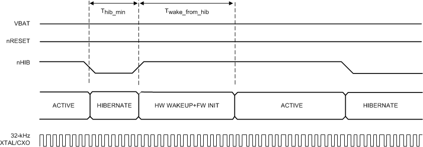
GUID-EB4B6C4F-7387-4997-AC36-CB6FC99EFBED-low.gifFigure 8-7 nHIB Timing Diagram
Note:

The internal 32.768-kHz XTAL is kept enabled by default when the chip goes into HIBERNATE mode in response to nHIB being pulled low.


Table 8-8 describes the timing requirements for nHIB.

Table 8-8 nHIB Timing Requirements
ITEMNAMEDESCRIPTIONMINTYPMAXUNIT
Thib_minMinimum hibernate timeMinimum pulse width of nHIB being low(1)10ms
Twake_from_hibHardware wakeup time plus firmware initialization timeSee(2)50ms
If temperature changes by more than 20°C, initialization time from HIB can increase by 200 ms due to radio calibration.
Ensure that the nHIB pulse width is kept above the minimum requirement under all conditions (such as power up, MCU reset, and so on).