ZHCS477K September   2011  – August 2022 BQ294502 , BQ294504 , BQ294506 , BQ294512 , BQ294522 , BQ294524 , BQ294532 , BQ294533 , BQ294534 , BQ294582 , BQ294592

PRODUCTION DATA  

  1. 特性
  2. 应用
  3. 说明
  4. Revision History
  5. Device Comparison Table
  6. Pin Configuration and Functions
  7. Specifications
    1. 7.1 Absolute Maximum Ratings
    2. 7.2 ESD Ratings
    3. 7.3 Recommended Operating Conditions
    4. 7.4 Thermal Information
    5. 7.5 Electrical Characteristics
    6. 7.6 Typical Characteristics
  8. Detailed Description
    1. 8.1 Overview
    2. 8.2 Functional Block Diagram
    3. 8.3 Feature Description
      1. 8.3.1 Sense Positive Input for VX
      2. 8.3.2 Output Drive, OUT
      3. 8.3.3 Supply Input, VDD
      4. 8.3.4 Thermal Pad, PWRPAD
    4. 8.4 Device Functional Modes
      1. 8.4.1 NORMAL Mode
      2. 8.4.2 OVERVOLTAGE Mode
      3. 8.4.3 Customer Test Mode
  9. Application and Implementation
    1. 9.1 Application Information
    2. 9.2 Typical Application
      1. 9.2.1 Design Requirements
      2. 9.2.2 Detailed Design Procedure
      3. 9.2.3 Application Curves
    3. 9.3 System Examples
  10. 10Power Supply Recommendations
  11. 11Layout
    1. 11.1 Layout Guidelines
    2. 11.2 Layout Example
  12. 12Device and Documentation Support
    1. 12.1 Device Support
      1. 12.1.1 第三方产品免责声明
    2. 12.2 Related Documentation
    3. 12.3 Receiving Notification of Documentation Updates
    4. 12.4 支持资源
    5. 12.5 Trademarks
    6. 12.6 Electrostatic Discharge Caution
    7. 12.7 术语表
  13. 13Mechanical, Packaging, and Orderable Information

封装选项

机械数据 (封装 | 引脚)
散热焊盘机械数据 (封装 | 引脚)
订购信息

Customer Test Mode

Customer Test Mode (CTM) helps to reduce test time for checking the overvoltage delay timer parameter once the circuit is implemented in the battery pack. To enter CTM, set VDD to at least 10 V higher than V3 (see Figure 8-2). The delay timer is greater than 10 ms, but considerably shorter than the timer delay in normal operation. To exit CTM, remove the VDD to VC3 voltage differential of 10 V so that the decrease in this value automatically causes an exit.

CAUTION:

Avoid exceeding any Absolute Maximum Voltages on any pins when placing the part into CTM. Also avoid exceeding Absolute Maximum Voltages for the individual cell voltages (V3–V2), (V2–V1), and (V1–VSS). Stressing the pins beyond the rated limits may cause permanent damage to the device.

Figure 8-2 shows the timing for CTM.
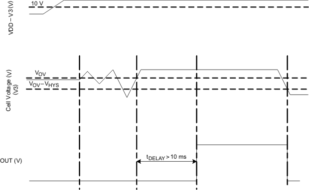
GUID-DB10A5DA-73DF-44F8-8D73-98792EE0BD59-low.gifFigure 8-2 Timing for Customer Test Mode

Figure 8-3 shows the measurement for current consumption for the product for both VDD and Vx.
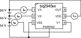
GUID-CF473F34-C66A-4847-A618-2C002A0E7CEF-low.gifFigure 8-3 Configuration for IC Current Consumption Test