ZHCS477K September   2011  – August 2022 BQ294502 , BQ294504 , BQ294506 , BQ294512 , BQ294522 , BQ294524 , BQ294532 , BQ294533 , BQ294534 , BQ294582 , BQ294592

PRODUCTION DATA  

  1. 特性
  2. 应用
  3. 说明
  4. Revision History
  5. Device Comparison Table
  6. Pin Configuration and Functions
  7. Specifications
    1. 7.1 Absolute Maximum Ratings
    2. 7.2 ESD Ratings
    3. 7.3 Recommended Operating Conditions
    4. 7.4 Thermal Information
    5. 7.5 Electrical Characteristics
    6. 7.6 Typical Characteristics
  8. Detailed Description
    1. 8.1 Overview
    2. 8.2 Functional Block Diagram
    3. 8.3 Feature Description
      1. 8.3.1 Sense Positive Input for VX
      2. 8.3.2 Output Drive, OUT
      3. 8.3.3 Supply Input, VDD
      4. 8.3.4 Thermal Pad, PWRPAD
    4. 8.4 Device Functional Modes
      1. 8.4.1 NORMAL Mode
      2. 8.4.2 OVERVOLTAGE Mode
      3. 8.4.3 Customer Test Mode
  9. Application and Implementation
    1. 9.1 Application Information
    2. 9.2 Typical Application
      1. 9.2.1 Design Requirements
      2. 9.2.2 Detailed Design Procedure
      3. 9.2.3 Application Curves
    3. 9.3 System Examples
  10. 10Power Supply Recommendations
  11. 11Layout
    1. 11.1 Layout Guidelines
    2. 11.2 Layout Example
  12. 12Device and Documentation Support
    1. 12.1 Device Support
      1. 12.1.1 第三方产品免责声明
    2. 12.2 Related Documentation
    3. 12.3 Receiving Notification of Documentation Updates
    4. 12.4 支持资源
    5. 12.5 Trademarks
    6. 12.6 Electrostatic Discharge Caution
    7. 12.7 术语表
  13. 13Mechanical, Packaging, and Orderable Information

封装选项

机械数据 (封装 | 引脚)
散热焊盘机械数据 (封装 | 引脚)
订购信息

Feature Description

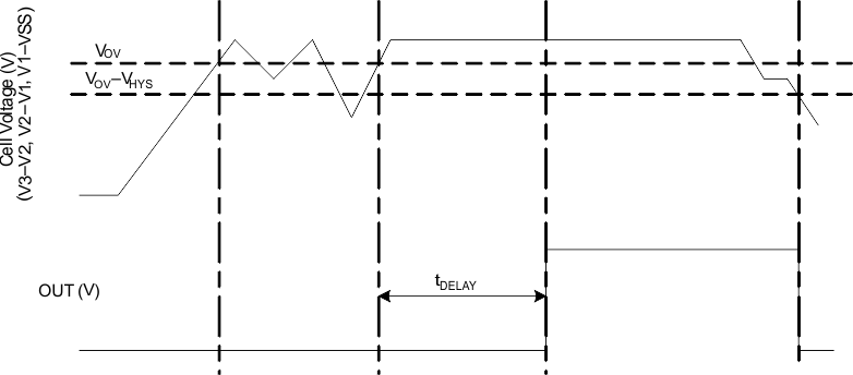
The voltage sensing for each cell is done independently using a multiplexer. The method of overvoltage detection is comparing the voltage to an overvoltage protection voltage VOV. Once the voltage exceeds the programmed fixed value, the delay timer circuit is activated. This delay (tDELAY) is fixed for either a 4-s or 6.5-s delay. When these conditions are satisfied, the OUT terminal is transitioned to a high level. This output (OUT) is released to a low condition if all of the cell inputs (Vx) are below the OVP threshold minus the Vhys.
GUID-C4E63CB3-28B8-498E-90DF-BF2EB82D11C2-low.gifFigure 8-1 Timing for Overvoltage Sensing