ZHCSLN5D december 2010 – september 2020 BQ24133
PRODUCTION DATA
- 1
- 1 特性
- 2 应用
- 3 说明
- 4 Revision History
- 5 Description (continued)
- 6 Device Comparison Table
- 7 Pin Configuration and Functions
- 8 Specifications
-
9 Detailed Description
- 9.1 Overview
- 9.2 Functional Block Diagram
- 9.3
Feature Description
- 9.3.1 Battery Voltage Regulation
- 9.3.2 Battery Current Regulation
- 9.3.3 Battery Precharge Current Regulation
- 9.3.4 Input Current Regulation
- 9.3.5 Charge Termination, Recharge, And Safety Timers
- 9.3.6 Power Up
- 9.3.7 Input Undervoltage Lockout (UVLO)
- 9.3.8 Input Overvoltage/Undervoltage Protection
- 9.3.9 Enable and Disable Charging
- 9.3.10 System Power Selector
- 9.3.11 Converter Operation
- 9.3.12 Automatic Internal Soft-Start Charger Current
- 9.3.13 Charge Overcurrent Protection
- 9.3.14 Charge Undercurrent Protection
- 9.3.15 Battery Detection
- 9.3.16 Battery Short Protection
- 9.3.17 Battery Overvoltage Protection
- 9.3.18 Temperature Qualification
- 9.3.19 MOSFET Short Circuit and Inductor Short Circuit Protection
- 9.3.20 Thermal Regulation and Shutdown Protection
- 9.3.21 Timer Fault Recovery
- 9.3.22 Charge Status Outputs
- 9.4 Device Functional Modes
- 10Application and Implementation
- 11Power Supply Recommendations
- 12Layout
- 13Device and Documentation Support
- 14Mechanical, Packaging, and Orderable Information
8.6 Typical Characteristics
Table 8-1 Table of Graphs(1)
| FIGURE | DESCRIPTION | |||
|---|---|---|---|---|
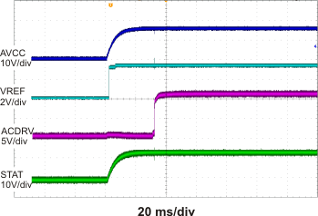
| Figure 8-1 | AVCC, VREF, ACDRV and STAT Power Up (ISET=0) | |||
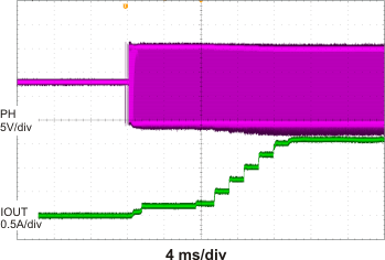
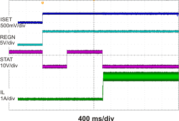
| Figure 8-2 | Charge Enable by ISET | |||
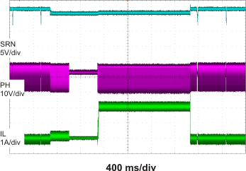
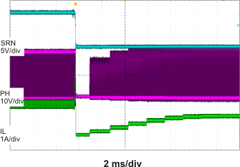
| Figure 8-3 | Current Soft Start | |||
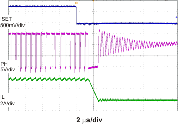
| Figure 8-4 | Charge Disable by ISET | |||
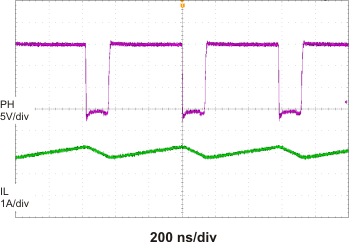
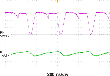
| Figure 8-5 | Continuous Conduction Mode Switching | |||
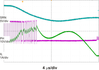
| Figure 8-6 | Discontinuous Conduction Mode Switching | |||
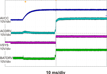
| Figure 8-7 | BATFET to ACFET Transition during Power Up | |||
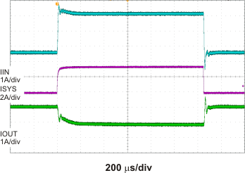
| Figure 8-8 | System Load Transient (Input Current DPM) | |||
| Figure 8-9 | Battery Insertion and Removal | |||
| Figure 8-10 | Battery to Ground Short Protection | |||
| Figure 8-11 | Battery to Ground Short Transition | |||
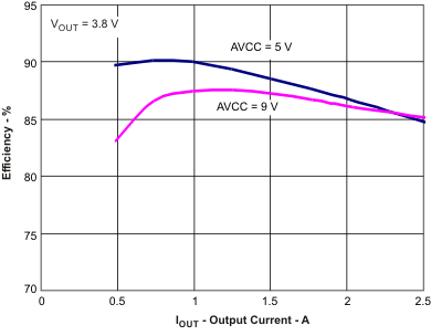
| Figure 8-12 | Efficiency vs Output Current (VOUT = 3.8 V) | |||
| Figure 10-4 | Efficiency vs Output Current (2-3 cell) | |||
(1) All waveforms and data are measured on HPA715 EVM.
