ZHCSLN5D december 2010 – september 2020 BQ24133
PRODUCTION DATA
- 1
- 1 特性
- 2 应用
- 3 说明
- 4 Revision History
- 5 Description (continued)
- 6 Device Comparison Table
- 7 Pin Configuration and Functions
- 8 Specifications
-
9 Detailed Description
- 9.1 Overview
- 9.2 Functional Block Diagram
- 9.3
Feature Description
- 9.3.1 Battery Voltage Regulation
- 9.3.2 Battery Current Regulation
- 9.3.3 Battery Precharge Current Regulation
- 9.3.4 Input Current Regulation
- 9.3.5 Charge Termination, Recharge, And Safety Timers
- 9.3.6 Power Up
- 9.3.7 Input Undervoltage Lockout (UVLO)
- 9.3.8 Input Overvoltage/Undervoltage Protection
- 9.3.9 Enable and Disable Charging
- 9.3.10 System Power Selector
- 9.3.11 Converter Operation
- 9.3.12 Automatic Internal Soft-Start Charger Current
- 9.3.13 Charge Overcurrent Protection
- 9.3.14 Charge Undercurrent Protection
- 9.3.15 Battery Detection
- 9.3.16 Battery Short Protection
- 9.3.17 Battery Overvoltage Protection
- 9.3.18 Temperature Qualification
- 9.3.19 MOSFET Short Circuit and Inductor Short Circuit Protection
- 9.3.20 Thermal Regulation and Shutdown Protection
- 9.3.21 Timer Fault Recovery
- 9.3.22 Charge Status Outputs
- 9.4 Device Functional Modes
- 10Application and Implementation
- 11Power Supply Recommendations
- 12Layout
- 13Device and Documentation Support
- 14Mechanical, Packaging, and Orderable Information
9.3.4 Input Current Regulation
The total input current from an AC adapter or other DC sources is a function of the system supply current and the battery charging current. System current normally fluctuated as portions of the systems are powered up or down. Without Dynamic Power Management (DPM), the source must be able to supply the maximum system current and the maximum available charger input current simultaneously. By using DPM, the input current regulator reduces the charging current when the summation of system power and charge power exceeds the maximum input power. Therefore, the current capability of the AC adapter can be lowered, reducing system cost.
Input current is set by the voltage on ACSET pin using the following equation:
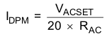
The ACP and ACN pins are used to sense across RAC with default value of 20 mΩ. However, resistors of other values can also be used. A larger sense resistor will give a larger sense voltage and higher regulation accuracy, at the expense of higher conduction loss.