ZHCSLN5D december 2010 – september 2020 BQ24133
PRODUCTION DATA
- 1
- 1 特性
- 2 应用
- 3 说明
- 4 Revision History
- 5 Description (continued)
- 6 Device Comparison Table
- 7 Pin Configuration and Functions
- 8 Specifications
-
9 Detailed Description
- 9.1 Overview
- 9.2 Functional Block Diagram
- 9.3
Feature Description
- 9.3.1 Battery Voltage Regulation
- 9.3.2 Battery Current Regulation
- 9.3.3 Battery Precharge Current Regulation
- 9.3.4 Input Current Regulation
- 9.3.5 Charge Termination, Recharge, And Safety Timers
- 9.3.6 Power Up
- 9.3.7 Input Undervoltage Lockout (UVLO)
- 9.3.8 Input Overvoltage/Undervoltage Protection
- 9.3.9 Enable and Disable Charging
- 9.3.10 System Power Selector
- 9.3.11 Converter Operation
- 9.3.12 Automatic Internal Soft-Start Charger Current
- 9.3.13 Charge Overcurrent Protection
- 9.3.14 Charge Undercurrent Protection
- 9.3.15 Battery Detection
- 9.3.16 Battery Short Protection
- 9.3.17 Battery Overvoltage Protection
- 9.3.18 Temperature Qualification
- 9.3.19 MOSFET Short Circuit and Inductor Short Circuit Protection
- 9.3.20 Thermal Regulation and Shutdown Protection
- 9.3.21 Timer Fault Recovery
- 9.3.22 Charge Status Outputs
- 9.4 Device Functional Modes
- 10Application and Implementation
- 11Power Supply Recommendations
- 12Layout
- 13Device and Documentation Support
- 14Mechanical, Packaging, and Orderable Information
Pin Functions
| PIN | TYPE | DESCRIPTION | |
|---|---|---|---|
| NAME | NO. | ||
| ACDRV | 8 | O | AC adapter to system switch driver output. Connect to 4-kΩ resistor then to the gate of the ACFET N-channel power MOSFET and the reverse conduction blocking N-channel power MOSFET. Connect both FETs as common-source. The internal gate drive is asymmetrical, allowing a quick turnoff and slower turnon in addition to the internal break-before-make logic with respect to the BATDRV. |
| ACN | 5 | I | Adapter current sense resistor negative input. A 0.1-µF ceramic capacitor is placed from ACN to ACP to provide differential-mode filtering. An optional 0.1-µF ceramic capacitor is placed from ACN pin to AGND for common-mode filtering. |
| ACP | 6 | P/I | Adapter current sense resistor positive input. A 0.1-µF ceramic capacitor is placed from ACN to ACP to provide differential-mode filtering. A 0.1-µF ceramic capacitor is placed from ACP pin to AGND for common-mode filtering. |
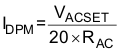
| ACSET | 17 | I | Input current set point. Use a voltage divider from VREF to ACSET to AGND to set this value:
 |
| AGND | Thermal Pad | P | Exposed pad beneath the IC. Always solder Thermal Pad to the board, and have vias on the Thermal Pad plane star-connecting to AGND and ground plane for high-current power converter. It dissipates the heat from the IC. |
| AVCC | 4 | P | IC power positive supply. Place a 1-µF ceramic capacitor from AVCC to AGND and place it as close as possible to IC. Place a 10-Ω resistor from input side to AVCC pin to filter the noise. For 5-V input, a 5-Ω resistor is recommended. |
| BATDRV | 19 | O | Battery discharge MOSFET gate driver output. Connect to 1-kΩ resistor to the gate of the BATFET P-channel power MOSFET. Connect the source of the BATFET to the system load voltage node. Connect the drain of the BATFET to the battery pack positive node. The internal gate drive is asymmetrical to allow a quick turnoff and slower turnon, in addition to the internal break-before-make logic with respect to ACDRV. |
| BTST | 21 | P | PWM high-side driver positive supply. Connect the 0.047-µF bootstrap capacitor from SW to BTST. |
| CELL | 14 | I | Cell selection pin. Set CELL pin LOW for 1-cell, Float for 2-cell (0.8 V - 1.8 V), and HIGH for 3-cell with a fixed 4.2 V per cell. |
| CMSRC | 7 | O | Connect to common source of N-channel ACFET and reverse blocking MOSFET (RBFET). Place 4-kΩ resistor from CMSRC pin to the common source of ACFET and RBFET to control the turnon speed. The resistance between ACDRV and CMSRC should be 500 kΩ or bigger. |
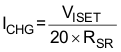
| ISET | 13 | I | Fast charge current set point. Use a voltage divider from VREF to ISET to AGND to set the fast charge current:
 |
| OVPSET | 18 | I | Valid input voltage set point. Use a voltage divider from input to OVPSET to AGND to set this voltage. The voltage above internal 1.6-V reference indicates input overvoltage, and the voltage below internal 0.5-V reference indicates input undervoltage. In either condition, charge terminates, and input NMOS pair ACFET/RBFET turn off. LED driven by STAT pin keeps blinking, reporting fault condition. |
| PGND | 22, 23 | P | Power ground. Ground connection for high-current power converter node. On PCB layout, connect directly to ground connection of input and output capacitors of the charger. Only connect to AGND through the Thermal Pad underneath the IC. |
| PVCC | 2, 3 | P | Charger input voltage. Connect at least 10-µF ceramic capacitor from PVCC to PGND and place it as close as possible to IC. |
| REGN | 20 | P | PWM low-side driver positive 6-V supply output. Connect a 1-μF ceramic capacitor from REGN to PGND pin, close to the IC. Generate high-side driver bootstrap voltage by integrated diode from REGN to BTST. |
| SRN | 15 | I | Charge current sense resistor negative input. A 0.1-μF ceramic capacitor is placed from SRN to SRP to provide differential-mode filtering. A 0.1-μF ceramic capacitor is placed from SRN pin to AGND for common-mode filtering. |
| SRP | 16 | I/P | Charge current sense resistor, positive input. A 0.1-μF ceramic capacitor is placed from SRN to SRP to provide differential-mode filtering. A 0.1-μF ceramic capacitor is placed from SRP pin to AGND for common-mode filtering. |
| STAT | 9 | O | Open-drain charge status pin with 10-kΩ pullup to power rail. The STAT pin can be used to drive LED or communicate with the host processor. It indicates various charger operations: LOW when charge in progress. HIGH when charge is complete or in SLEEP mode. Blinking at 0.5 Hz when fault occurs, including charge suspend, input overvoltage, timer fault and battery absent. |
| SW | 1, 24 | P | Switching node, charge current output inductor connection. Connect the 0.047-µF bootstrap capacitor from SW to BTST. |
| TS | 10 | I | Temperature qualification voltage input. Connect a negative temperature coefficient thermistor. Program the hot and cold temperature window with a resistor divider from VREF to TS to AGND. The temperature qualification window can be set to 5-40°C or wider. The 103AT thermistor is recommended. |
| TTC | 11 | I | Safety Timer and termination control. Connect a capacitor from this node to AGND to set the fast charge safety timer(5.6 min/nF). Precharge timer is internally fixed to 30 minutes. Pull the TTC to LOW to disable the charge termination and safety timer. Pull the TTC to HIGH to disable the safety timer but allow the charge termination. |
| VREF | 12 | P | 3.3-V reference voltage output. Place a 1-μF ceramic capacitor from VREF to AGND pin close to the IC. This voltage could be used for programming ISET and ACSET and TS pins. It may also serve as the pullup rail of STAT pin and CELL pin. |