SLUS784E December 2007 – December 2015
PRODUCTION DATA.
- 1 Features
- 2 Applications
- 3 Description
- 4 Revision History
- 5 Device Options
- 6 Pin Configuration and Functions
- 7 Specifications
-
8 Detailed Description
- 8.1 Overview
- 8.2 Functional Block Diagram
- 8.3
Feature Description
- 8.3.1 Control Logic Overview
- 8.3.2 Temperature Qualification (Applies Only to Versions With TS Pin Option)
- 8.3.3 Input Overvoltage Detection, Power Good Status Output
- 8.3.4 Charge Status Outputs
- 8.3.5 Battery Charging: Constant Current Phase
- 8.3.6 Charge Current Translator
- 8.3.7 Battery Voltage Regulation
- 8.3.8 Pre-Charge Timer
- 8.3.9 Thermal Protection Loop
- 8.3.10 Thermal Shutdown And Protection
- 8.3.11 Dynamic Timer Function
- 8.3.12 Charge Termination Detection and Recharge
- 8.3.13 Battery Absent Detection - Voltage Mode Algorithm
- 8.3.14 Charge Safety Timer
- 8.3.15 Short-Circuit Protection
- 8.3.16 Startup With Deeply Depleted Battery Connected
- 8.4 Device Functional Modes
- 9 Application and Implementation
- 10Power Supply Recommendations
- 11Layout
- 12Device and Documentation Support
- 13Mechanical, Packaging, and Orderable Information
封装选项
请参考 PDF 数据表获取器件具体的封装图。
机械数据 (封装 | 引脚)
- DRC|10
散热焊盘机械数据 (封装 | 引脚)
- DRC|10
订购信息
6 Pin Configuration and Functions
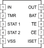
bq24085 DRC Package
10-Pin VSON
Top View

bq24087 DRC Package
10-Pin VSON
Top View

Pin Functions
| PIN | I/O | DESCRIPTION | |||
|---|---|---|---|---|---|
| NAME | bq24086/8 | bq24085 | bq24087 | ||
| BAT | 9 | 9 | 9 | I | Battery voltage sense input. Connect to the battery positive terminal. Connect a 390-Ω resistor from BAT to OUT for I(OUT) < 200 mA. |
| CE | – | 8 | 7 | I | Charge enable input. CE = LO enables charger. CE = HI disables charger. |
| IN | 1 | 1 | 1 | I | Charge input voltage and internal supply. Connect a 1-μF (minimum) capacitor from IN to VSS. CIN ≥ COUT |
| ISET | 6 | 6 | 6 | O | Charge current set point, resistor connected from ISET to VSS sets charge current value. Connect a 0.1-μF capacitor from BAT to ISET for I(OUT) < 200 mA. |
| OUT | 10 | 10 | 10 | O | Charge current output. Connect to the battery positive terminal. Connect a 1-μF (minimum) capacitor from OUT to VSS. |
| PG | 7 | 7 | O | Power good status output (open-collector), active low. | |
| STAT1 | 3 | 3 | 3 | O | Charge status output 1 (open-collector, see Table 3). |
| STAT2 | 4 | 4 | 4 | O | Charge status output 2 (open-collector, see Table 3). |
| TE | – | – | 8 | I | Termination enable input. TE = LO enables termination detection and battery absent detection. TE = HI disables termination detection and battery absent detection. |
| TMR | 2 | 2 | 2 | I | Safety timer program input, timer disabled if floating. Connect a resistor to VSS pin to program safety timer timeout value. |
| TS | 8 | – | – | I | Temperature sense input, connect to battery pack thermistor. Connect an external resistive divider to program temperature thresholds. |
| VSS | 5 | 5 | 5 | I | Ground |
| Exposed Thermal Pad | Pad | Pad | Pad | – | There is an internal electrical connection between the exposed thermal pad and Vss pin of the IC. The exposed thermal pad must be connected to the same potential as the VSS pin on the printed circuit board. Do not use the thermal pad as the primary ground input for the IC. VSS pin must be connected to ground at all times. |
