SLUS784E December 2007 – December 2015
PRODUCTION DATA.
- 1 Features
- 2 Applications
- 3 Description
- 4 Revision History
- 5 Device Options
- 6 Pin Configuration and Functions
- 7 Specifications
-
8 Detailed Description
- 8.1 Overview
- 8.2 Functional Block Diagram
- 8.3
Feature Description
- 8.3.1 Control Logic Overview
- 8.3.2 Temperature Qualification (Applies Only to Versions With TS Pin Option)
- 8.3.3 Input Overvoltage Detection, Power Good Status Output
- 8.3.4 Charge Status Outputs
- 8.3.5 Battery Charging: Constant Current Phase
- 8.3.6 Charge Current Translator
- 8.3.7 Battery Voltage Regulation
- 8.3.8 Pre-Charge Timer
- 8.3.9 Thermal Protection Loop
- 8.3.10 Thermal Shutdown And Protection
- 8.3.11 Dynamic Timer Function
- 8.3.12 Charge Termination Detection and Recharge
- 8.3.13 Battery Absent Detection - Voltage Mode Algorithm
- 8.3.14 Charge Safety Timer
- 8.3.15 Short-Circuit Protection
- 8.3.16 Startup With Deeply Depleted Battery Connected
- 8.4 Device Functional Modes
- 9 Application and Implementation
- 10Power Supply Recommendations
- 11Layout
- 12Device and Documentation Support
- 13Mechanical, Packaging, and Orderable Information
封装选项
请参考 PDF 数据表获取器件具体的封装图。
机械数据 (封装 | 引脚)
- DRC|10
散热焊盘机械数据 (封装 | 引脚)
- DRC|10
订购信息
8 Detailed Description
8.1 Overview
The charge current is programmable using external components (RISET resistor). The charge process starts when an external input power is connected to the system, the charger is enabled by CE = LO and the battery voltage is below the recharge threshold, V(BAT) < V(RCH). When the charge cycle starts a safety timer is activated, if the safety timer function is enabled. The safety timer timeout value is set by an external resistor connected to TMR pin.
When the charger is enabled two control loops modulate the battery switch drain to source impedance to limit the BAT pin current to the programmed charge current value (charge current loop) or to regulate the BAT pin voltage to the programmed charge voltage value (charge voltage loop). If V(BAT) < V(LOWV) (3 V typical) the BAT pin current is internally set to 10% of the programmed charge current value.
A typical charge profile for an operation condition that does not cause the IC junction temperature to exceed TJ(REG), (112°C typical), is shown in Figure 8.
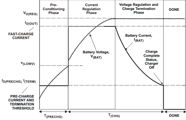 Figure 8. Charging Profile With TJ(REG)
If the operating conditions cause the IC junction temperature to exceed TJ(REG), the charge cycle is modified, with the activation of the integrated thermal control loop. The thermal control loop is activated when a internal junction temperature monitoring voltage is lower than a fixed, temperature stable internal voltage. The junction temperature monitoring voltage is inversely proportional to the IC junction temperature. The thermal loop overrides the other charger control loops and reduces the charge current until the IC junction temperature returns to TJ(REG), effectively regulating the IC junction temperature.
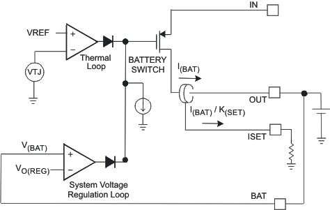 Figure 9. Thermal Regulation Circuit
A modified charge cycle, with the thermal loop active, is shown in Figure 10.
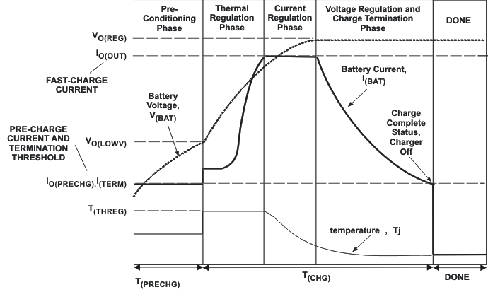 Figure 10. Charge Profile, Thermal Loop Active
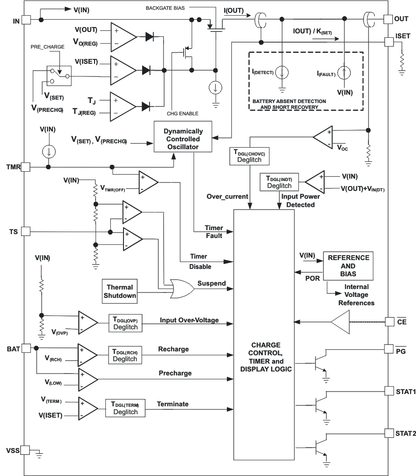
8.2 Functional Block Diagram
8.3 Feature Description
8.3.1 Control Logic Overview
An external host can enable or disable the charging process by using a dedicated control pin, CE. A low-level signal on this pin enables the charge, and a high-level signal disables the charge. The bq24085/6/7/8 is in stand-by mode with CE = HI. When the charger function is enabled (CE = LO) a new charge is initiated.
Table 1 describes the charger control logic operation. In bq24085/6/7/8, the pack temperature status is internally set to OK without the TS pin.
Table 1. Control Logic Functionality
| bq24085/6/7/8 OPERATION MODE | CE | INPUT POWER | TIMER FAULT (latched) | OUTPUT SHORT CIRCUIT | TERMINATION (latched) | PACK TEMP | THERMAL SHUTDOWN | POWER DOWN | CHARGER POWER STAGE |
|---|---|---|---|---|---|---|---|---|---|
| POWER DOWN | LO | Low | X | X | X | X | X | Yes | OFF |
| SLEEP | X | Not Detected | X | X | X | X | X | No | OFF |
| STANDBY | HI | Detected | X | X | X | X | X | No | OFF |
| SEE STATE DIAGRAM | LO | Detected | X | Yes | X | X | X | No | |
| LO | Detected | No | No | Yes | X | X | No | OFF | |
| LO | Detected | Yes | No | No | X | X | No | IFAULT | |
| LO | Detected | No | No | Yes | Absent | TJ < TSHUT | No | IDETECT | |
| LO | Detected | No | No | No | Hot or Cold | TJ < TSHUT | No | OFF | |
| LO | Detected | No | No | No | Ok | TJ < TSHUT | No | OFF | |
| LO | Over Voltage | No | No | No | Ok | TJ < TSHUT | No | OFF | |
| CHARGING | LO | Detected | No | No | No | Ok | TJ < TSHUT | No | ON |
In both STANDBY and SUSPEND modes the charge process is disabled. In the STANDBY mode all timers are reset; in SUSPEND mode the timers are held at the count stored when the suspend mode was set.
The timer fault, termination and output short circuit variables shown in the control logic table are latched in the detection circuits, outside the control logic. Refer to the Pre-Charge Timer, Dynamic Timer Function, Charge Safety Timer, Charge Termination Detection and Recharge, and Short-Circuit Protection sections for additional details on how those latched variables are reset.
8.3.2 Temperature Qualification (Applies Only to Versions With TS Pin Option)
The bq24085/6/7/8 devices continuously monitor the battery temperature by measuring the voltage between the TS and VSS pins. The IC compares the voltage on the TS pin against the internal V(TS1) and V(TS2) thresholds to determine if charging is allowed. Once a temperature outside the V(TS1) and V(TS2) thresholds is detected, the IC immediately suspends the charge. The IC suspends charge by turning off the power FET and holding the timer value (that is, timers are NOT reset). Charge is resumed when the temperature returns to the normal range.
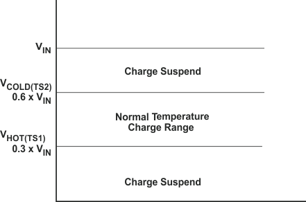 Figure 11. Battery Temperature Qualification With NTC Thermistor
The external resistors RT1 and RT2 (see Figure 18) enable selecting a temperature window. If RTC and RTH are the thermistor impedances for the Cold and Hot thresholds the values for RT1 and RT2 can be calculated as follows for a NTC (negative temperature coefficient) thermistor. Solve for RT2 first and substitute into RT1 equation. RTC and RTH can be found in the NTC thermistor datasheet specification.


Applying a fixed voltage, 1/2 Vin (50% resistor divider from Vin to ground), to the TS pin to disable the temperature sensing feature.
8.3.3 Input Overvoltage Detection, Power Good Status Output
The input power detection status for pin IN is shown at the open collector output pin PG.
Table 2. Input Power Detection Status
| INPUT POWER DETECTION (IN) | PG STATE |
|---|---|
| NOT DETECTED | High impedance |
| DETECTED, NO OVERVOLTAGE | LO |
| DETECTED, OVERVOLTAGE | High impedance |
The bq24085/6/7/8 detects an input overvoltage when V(IN) > V(OVP). When an overvoltage protection is detected the charger function is turned off and the bq24085/6/7/8 is set to standby mode of operation. Since the OVP detection is not latched, the IC returns to normal operation when fault condition is removed.
8.3.4 Charge Status Outputs
The open-collector STAT1 and STAT2 outputs indicate various charger operations as shown in Table 3. These status pins can be used to drive LEDs or communicate to the host processor.
NOTE
OFF indicates the open-collector transistor is turned off. When termination is disabled (TMR pin floating, or TE = Hi for bq24087) the Done state is not available; the status LEDs indicate fast charge if V(BAT) > V(LOWV) and precharge if V(BAT) < V(LOWV). The available output current is a function of the OUT pin voltage, See Figure 16.
Table 3. Charge Status(1)
| Charge State | STAT1 | STAT2 |
|---|---|---|
| Precharge in progress | ON | ON |
| Fast charge in progress | ON | OFF |
| Done (termination enabled only) | OFF | ON |
| Charge Suspend (temperature) | OFF | OFF |
| Timer Fault | ||
| Charger off | ||
| Selected Input power overvoltage detected | ||
| Battery absent | ||
| Batteryshort |
8.3.5 Battery Charging: Constant Current Phase
The bq24085/6/7/8 family offers on-chip current regulation. The current regulation is defined by the value of the resistor connected to ISET pin.
During a charge cycle the fast charge current IO(OUT) is applied to the battery if the battery voltage is above the V(LOWV) threshold (2.95 V typical):

where
- K(SET) is the output current set factor and V(SET) is the output current set voltage.
During a charge cycle if the battery voltage is below the V(LOWV) threshold a pre-charge current I(PRECHG) is applied to the battery. This feature revives deeply discharged cells.

where
- K(SET) is the output current set factor and V(PRECHG) is the precharge set voltage.
At low constant current charge currents, less than 200 mA, TI recommends that a 0.1-μF capacitor be placed between the ISET and BAT pins to insure stability.
8.3.6 Charge Current Translator
When the charge function is enabled, internal circuits generate a current proportional to the charge current at the ISET pin. This current, when applied to the external charge current programming resistor RISET generates an analog voltage that can be monitored by an external host to calculate the current sourced from the OUT pin.

8.3.7 Battery Voltage Regulation
The battery pack voltage is sensed through the BAT pin, which is tied directly to the positive side of the battery pack. The bq24085/6/7/8 monitors the battery pack voltage between the BAT and VSS pins. When the battery voltage rises to VO(REG) threshold, the battery charging enters the voltage regulation phase, and charging current begins to taper down. The voltage regulation threshold VO(REG) is fixed by an internal IC voltage reference.
8.3.8 Pre-Charge Timer
The bq24085/6/7/8 family activates an internal safety timer during the battery pre-conditioning phase. The charge safety timer time-out value is set by the external resistor connected to TMR pin, RTMR, and the timeout constants K(PCHG) and t(CHG) :
The pre-charge timer operation is detailed in Table 4.
Table 4. Pre-Charge Timer Operational Modes
| bq24085/6/7/8 MODE | V(OUT) > V(LOWV) | PRE-CHARGE TIMER MODE |
|---|---|---|
| STANDBY (CE = Hi) | X | RESET |
| CHARGING | Yes | RESET |
| SUSPEND (TS out of range) | Yes | RESET |
| SUSPEND (TS out of range) | No | Hold |
| CHARGING, TMR PIN NOT OPEN | No | COUNTING, EXTERNAL PROGRAMMED RATE |
| CHARGING, TMR PIN OPEN | X | RESET |
In SUSPEND mode the pre-charge timer is put on hold (that is, pre-charge timer is not reset). Once normal operation resumes when the timer returns to the normal operating mode (COUNTING). If V(BAT) does not reach the internal voltage threshold V(LOWV) within the pre-charge timer period, a fault condition is detected. The charger is then turned off, and the pre-charge safety timer fault condition is latched.
When the pre-charge timer fault latch is set the charger is turned off. Under these conditions a small current IFAULT is applied to the OUT pin, as long as input power (IN) is detected AND V(OUT) < V(LOWV), as part of a timer fault recovery protocol. This current allows the output voltage to rise above the pre-charge threshold V(LOWV), resetting the pre-charge timer fault latch when the pack is removed. Table 5 further details the pre-charge timer fault latch operation.
Table 5. Pre-Charge Timer Latch Functionality
| PRE-CHARGE TIMER FAULT ENTERED WHEN | PRE-CHARGE TIMER FAULT LATCH RESET AT |
|---|---|
| Pre-charge timer timeout AND V(OUT) < V(LOW V) | CE rising edge or OVP detected |
| Input power removed (not detected) | |
| Timer function disabled |
8.3.9 Thermal Protection Loop
An internal control loop monitors the bq24085/6/7/8 junction temperature (TJ) to ensure safe operation during high power dissipations and increased ambient temperatures. This loop monitors the bq24085/6/7/8 junction temperature and reduces the charge current as necessary to keep the junction temperature from exceeding, TJ(REG), (112°C, typical).
The bq24085/6/7/8's thermal loop control can reduce the charging current down to approximately 105 mA if needed. If the junction temperature continues to rise, the IC will enter thermal shutdown.
8.3.10 Thermal Shutdown And Protection
Internal circuits monitor the junction temperature, TJ, of the die and suspends charging if TJ exceeds an internal threshold T(SHUT) (155°C typical). Charging resumes when TJ falls below the internal threshold T(SHUT) by approximately 20°C.
8.3.11 Dynamic Timer Function
The charge and pre-charge safety timers are programmed by the user to detect a fault condition if the charge cycle duration exceeds the total time expected under normal conditions. The expected charge time is usually calculated based on the fast charge current rate.
When the thermal loop is activated the charge current is reduced, and bq24085/6/7/8 activates the dynamic timer control. The dynamic timer control is an internal circuit that slows down the safety timer's clock frequency. The dynamic timer control circuit effectively extends the safety time duration for either the precharge or fast charge timer modes. This minimizes the chance of a safety timer fault due to thermal regulation.
The bq24085/6/7/8 dynamic timer control (DTC) monitors the voltage on pin ISET during pre-charge and fast charge, and if in thermal regulation slows the clock frequency proportionately to the change in charge current. The time duration is based on a 224 ripple counter, so slowing the clock frequency is a real time correction. The DTC circuit changes the safety timers clock period based on the V(SET)/V(ISET) ratio (fast charge) or V(PRECHG)/V(SET) ratio (pre-charge). Typical safety timer multiplier values relative to the V(SET)/V(ISET) ratio is shown in Figure 12 and Figure 13.
The device deglitch timers are set by the same oscillators as the safety and precharge timers. In thermal regulation, the timers are scaled appropriately, see Figure 2.
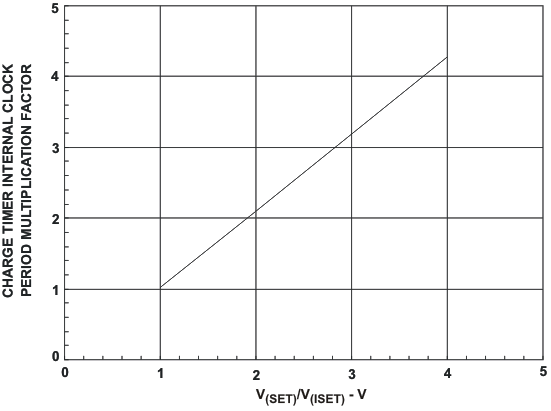 Figure 12. Safety Timer Linearity
Internal Clock Period Multiplication Factor
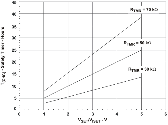 Figure 13. bq24085/6/78 Safety Timer Linearity for RTMR Values
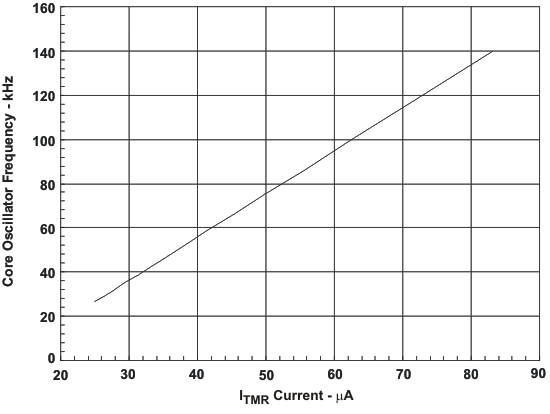 Figure 14. bq24085/6/7/8 Oscillator Linearity vs ITMR
RTMR 30 KΩ – 100 KΩ
8.3.12 Charge Termination Detection and Recharge
The charging current is monitored during the voltage regulation phase. Charge termination is indicated at the STATx pins (STAT1 = Hi-Z; STAT2 = Low ) once the charge current falls below the termination current threshold I(TERM). A deglitch period tDGL(TERM) is added to avoid false termination indication during transient events.
Charge termination is not detected if the charge current falls below the termination threshold as a result of the thermal loop activation. Termination is also not detected when charger enters the suspend mode, due to detection of invalid pack temperature or internal thermal shutdown.
Table 6 describes the termination latch functionality.
Table 6. Termination Latch Functionality
| TERMINATION DETECTED LATCHED WHEN | TERMINATION LATCH RESET AT |
|---|---|
| I(OUT) < I(TERM) AND t > tDGL(TERM) AND V(OUT) > V(RCH) | CE rising edge or OVP detected |
| New charging cycle started; see state diagram | |
| Termination disabled |
The termination function is DISABLED:
- In bq24085/6/7/8 the termination is disabled when the TMR pin is left open (floating).
- In bq24087, leaving the TMR pin open (floating) does not disable the termination. The only way to disabled termination in bq24087 is to have TE = high.
- Thermal regulation or thermal shutdown.
- Invalid battery pack temperature (TS fault).
8.3.13 Battery Absent Detection – Voltage Mode Algorithm
The bq24085/6/7/8 provides a battery absent detection scheme to reliably detect insertion and removal of battery packs. The detection circuit applies an internal current to the battery terminal, and detects battery presence based on the terminal voltage behavior. Figure 15 has a typical waveform of the output voltage when the battery absent detection is enabled and no battery is connected.
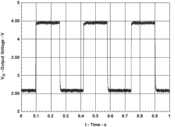 Figure 15. Battery-Absent Detection Waveforms
The battery absent detection function is disabled if the voltage at the BAT pin is held above the battery recharge threshold, V(RCH), after termination detection. When the voltage at the BAT pin falls to the recharge threshold, either by connection of a load to the battery or due to battery removal, the bq24085/6/7/8 begins a battery absent detection test. This test involves enabling a detection current, IDET(DOWN), for a period of t(DETECT) and checking to see if the battery voltage is below the pre-charge threshold, V(LOWV). Following this, the precharge current, IDET(UP) is applied for a period of t(DETECT) and the battery voltage checked again to be above the recharge threshold.
Passing both of the discharge and charging tests (battery terminal voltage being below the pre-charge and above the recharge thresholds on the battery detection test) indicates a battery absent fault at the STAT1 and STAT2 pins. Failure of either test starts a new charge cycle. For the absent battery condition, the voltage on the BAT pin rises and falls between the V(LOWV) and VO(REG) thresholds indefinitely. See the Operational Flow Chart, Figure 17, for more details on this algorithm. If it is desired to power a system load without a battery, TI recommends to float the TMR pin which puts the charger in LDO mode (disables termination).
The battery absent detection function is disabled when the termination is disabled.
After termination, the bq24085/6/7/8 provides a small battery leakage current, IBAT(DONE) (1 μA typical), to pull down the BAT pin voltage in the event of battery removal. If the leakage on the OUT pin is higher than this pulldown current, then the voltage at the pin remains above termination and a battery-absent state will not be detected. This problem is fixed with the addition of a pulldown resistor of 2 MΩ to 4 MΩ from the OUT pin to VSS. A resistor too small (< 2 MΩ) can cause the OUT pin voltage to drop below the V(LOWV) threshold before the recharge deglitch (typical 25 ms) expires, causing a fault condition. In this case, the bq24085/6/7/8 provides a fault current (typical 750 μA) to pull the pin above the termination threshold.
8.3.14 Charge Safety Timer
As a protection mechanism, the bq24085/6/7/8 has a user-programmable timer that monitors the total fast charge time. This timer (charge safety timer) is started at the beginning of the fast charge period. The safety charge timeout value is set by the value of an external resistor connected to the TMR pin (RTMR); if pin TMR is left open (floating) the charge safety timer is disabled.
Use Equation 7 to calculate the charge safety timer time-out value:
The safety timer operation modes are shown in Table 7
Table 7. Charge Safety Timer Operational Modes
| bq24085/6/7/8 | V(OUT) > V(LOWV) | CHARGE SAFETY TIMER MODE |
|---|---|---|
| STANDBY | X | RESET |
| CHARGING | No | RESET |
| SUSPEND | No | RESET |
| SUSPEND | Yes | SUSPEND |
| CHARGING, TMR PIN NOT OPEN | Yes | COUNTING |
| CHARGING, TMR PIN OPEN | X | RESET |
In SUSPEND mode, the charge safety timer is put on hold (that is, charge safety timer is not reset), normal operation resumes when the TS fault is removed and the timer returns to the normal operating mode (COUNTING). If charge termination is not reached within the timer period, a fault condition is detected. Under those circumstances, the LED status is updated to indicate a fault condition and the charger is turned off.
When the charge safety timer fault latch is set and the charger is turned off, a small current IFAULT is applied to the OUT pin, as long as input power (IN) is detected AND V(OUT) < V(RCHG), as part of a timer fault recovery protocol. This current allows the output voltage to rise above the recharge threshold V(RCHG) if the pack is removed, and assures that the charge safety timer fault latch is reset if the pack is removed and re-inserted. Table 8 further details the charge safety timer fault latch operation.
Table 8. Charge Safety Timer Latch Functionality
| CHARGE SAFETY TIMER FAULT ENTERED | CHARGE SAFETY TIMER FAULT LATCH RESET AT |
|---|---|
| V(OUT) > V(LOW V) | CE rising edge, or OVP detected |
| Input power removed (not detected) | |
| New charging cycle started; see state diagram |
8.3.15 Short-Circuit Protection
The internal comparators monitor the battery voltage and detect when a short circuit is applied to the battery terminal. If the voltage at the BAT pin is less than the internal threshold V(SCIND) (1.8 V typical), the STAT pins indicate a fault condition (STAT1 = STAT2 = Hi-Z). When the voltage at the BAT pin falls below a second internal threshold V(SC) (1.4 V typical), the charger power stage is turned off. A recovery current, I(SHORT) (15 mA typical), is applied to the BAT pin, enabling detection of the short circuit removal. The battery output current versus battery voltage is shown in the graph, Figure 16.
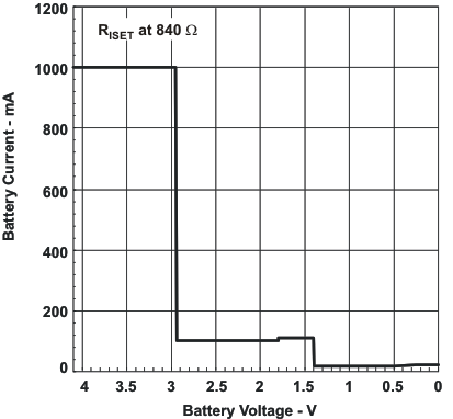 Figure 16. bq24085/6/7/8 Short Circuit Behavior
See the Application and Implementation section for additional details on start-up operation with V(BAT) < V(SC).
8.3.16 Startup With Deeply Depleted Battery Connected
The bq24085/6/7/8 charger furnishes the programmed charge current if a battery is detected. If no battery is connected the bq24085/6/7/8 operates as follows:
- The output current is limited to 15 mA (typical), if the voltage at BAT pin is below the short circuit detection threshold V(SC), 1.8 V typical.
- The output current is regulated to the programmed pre-charge current if V(SC) < V(BAT) < V(LOWV).
- The output current is regulated to the programmed fast charge current If V(BAT) > V(LOWV) AND voltage regulation is not reached.
The output voltage collapses if no battery is present and the end equipment requires a bias current larger than the available charge current.
8.4 Device Functional Modes
8.4.1 Power Down
The bq24085/6/7/8 family is in a power-down mode when the input power voltage (IN) is below the power-down threshold V(PDWN). During the power-down mode all IC functions are off, and the host commands at the control pins are not interpreted. The integrated power MOSFET connected between IN and OUT pins is off, the status output pins STAT1 and STAT2 are set to high impedance mode and PG output is set to the high impedance state.
8.4.2 Sleep Mode
The bq24085/6/7/8 enters the sleep mode when the input power voltage (IN) is above the power-down threshold V(PDWN) but still lower than the input power detection threshold, V(IN) < V(OUT) + VIN(DT).
During the sleep mode the charger is off, and the host commands at the control pins are not interpreted. The integrated power mosfet connected between IN and OUT pins is off, the status output pins STAT1 and STAT2 are set to the high impedance state and the PG output indicates input power not detected.
The sleep mode is entered from any other state, if the input power (IN) is not detected.
8.4.3 Overvoltage Lockout
The input power is detected when the input voltage V(IN) > V(OUT) + VIN(DT). When the input power is detected the bq24085/6/7/8 transitions from the sleep mode to the power-on-reset mode. In this mode of operation, an internal timer T(POR) is started and internal blocks are reset (power-on-reset). Until the timer expires, the STAT1 and STAT2 outputs indicate charger OFF, and the PG output indicates the input power status as not detected.
At the end of the power-on-reset delay, the internal comparators are enabled, and the STAT1, STAT2 and PG pins are active.
8.4.4 Stand-By Mode
In the bq24085/6/7/8, the stand-by mode is started at the end of the power-on-reset phase, if the input power is detected and CE = HI. In the stand-by mode, selected blocks in the IC are operational, and the control logic monitors system status and the control pins to define if the charger will be set to ON or OFF mode. The quiescent current required in stand-by mode is 100 μA typical.
If the CE pin is not available, the bq24085/6/7/8 enters the begin charge mode at the end of the power-on-reset phase.
8.4.5 Begin Charge Mode
All blocks in the IC are powered up, and the bq24085/6/7/8 is ready to start charging the battery pack. A new charge cycle is started when the control logic decides that all conditions required to enable a new charge cycle are met. During the begin charge phase all timers are reset, then the IC enters the charging mode.
8.4.6 Charging Mode
When the charging mode is active, the bq24085/6/7/8 executes the charging algorithm, as described in the Operational Flow Chart, Figure 17.
8.4.7 Suspend Mode
The suspend mode is entered when the pack temperature is not within the valid temperature range. During the suspend mode, the charger is set to OFF, but the timers are not reset.
The normal charging mode resumes when the pack temperature returns to the valid temperature range.
8.4.8 LDO Mode Operation
The LDO Mode (TMR pin open circuit) disables the charging termination circuit, disables the battery detect routine and holds the safety timer clock in reset. This is often used for operation without a battery or in production testing. This mode is different than a typical LDO since it has different modes of operation, and delivers less current at lower output voltages. See Figure 16 for the output current versus the output voltage.
NOTE
A load on the output prior to powering the device may keep the part in short-circuit mode. Also, during normal operation, exceeding the programmed fast charge level causes the output to drop, further restricting the output power, and soon ends up in short-circuit mode.
Operation with a battery or keeping the average load current below the programmed current level prevents this type of latch up. The OUT pin current can be monitored through the ISET pin. If the device is in LDO mode and battery is absent, TI recommends to use a 350-Ω feedback resistor between the BAT and OUT pins.
8.4.9 State Machine Diagram
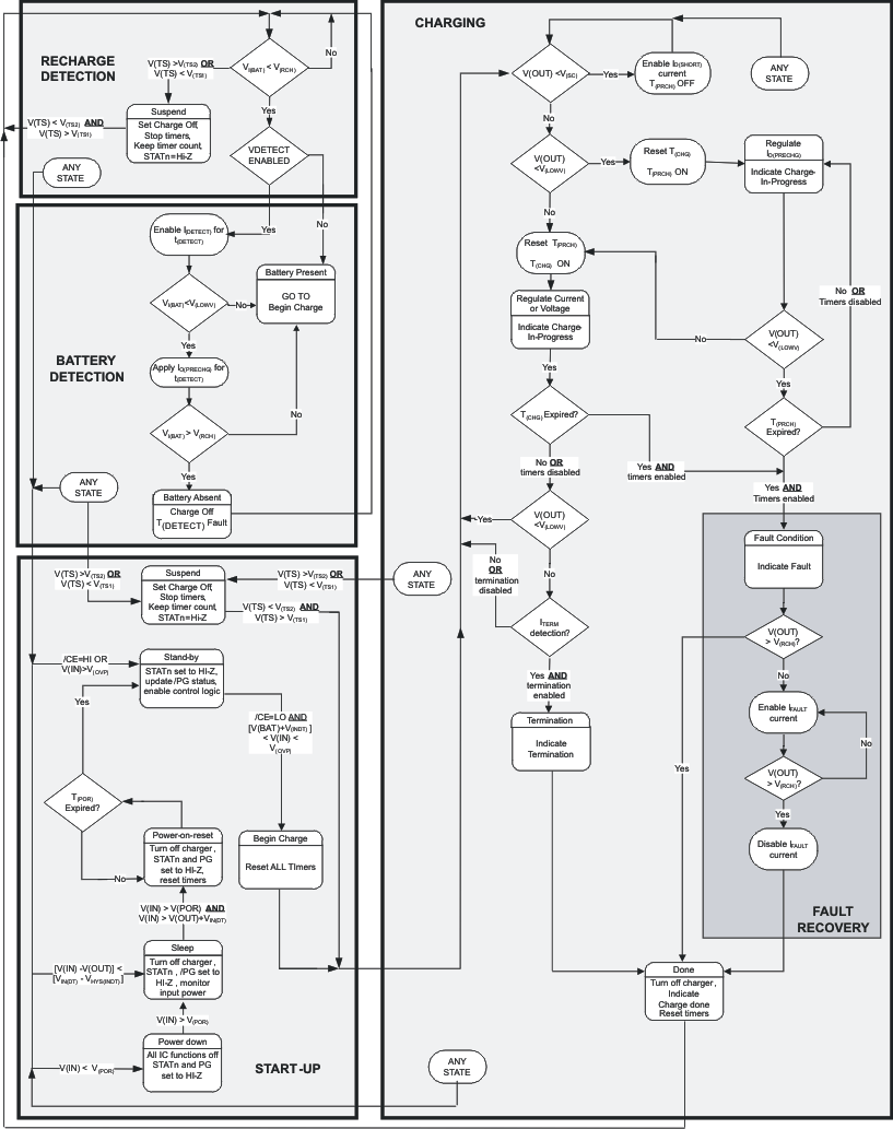 Figure 17. Operational Flow Chart