主要产品
电源管理器
时钟和计时器
数据转换器
热量与电源监控
|
TI Clock Solutions for FPGAs
TI's Clock products enables you to deliver high-performance, state-of-the-art products to market faster with lower risk and higher productivity. With a perfect blend of high performance, low power, high configurability clock devices that include clock jitter cleaners, clock generators and clock buffers we can support the complete clocking tree needs of FPGA's and enable them in moving to higher data rates for various data transmission standards.
Devices which address this need by providing low-noise precision clocks (<1ps RMS, 10kHz – 20MHz) for these type of applications. In addition, TI also provides clock devices that can help simplify and centralize the clock tree surrounding your FPGA, with fractional-N PLL-based generators and a wide portfolio of high-performance clock distribution buffers.
TI value your time and money in the search for the perfect clocking solution in race to win the market. TI has a diversified portfolio of Clock products to support all clocking needs. Some of the highlights of the portfolio are:
- High Performance: Address the clocking requirements for high-speed cores within FPGAs by providing low-noise precision clocks (<500 fs RMS, 10kHz – 20MHz)
Enables low EMI designs via SSC
- Simplify and Centralize: Provide solutions to simplify and centralize the clock tree surrounding FPGA, with Fractional-N PLL-based generators and a wide portfolio of high-performance clock distribution buffers
- Flexibility: Enable flexible frequency planning for FPGA customers by innovative architecture achieves many common communications frequencies simultaneously
Highly flexible and configurable devices to support a variety of different clock architectures.
- Integration: Highly integrated solution saves board space and cost by consolidating multiple oscillators.
Clock Generation
|
LMK03806 – Ultra-high Performance Clock Generator
 |
|
Parameter
|
LMK03806 - Ultra Low Jitter Clock Generator with 14 Programmable Outputs.
|
RMS Jitter (156.25 MHz), 1.875MHz to 20 MHz
|
57 fs, rms
|
| Number of inputs |
1x SE, DE, or crystal. |
|
Reference Frequency
|
SE or DE: 1 MHz to 500 MHz. Includes 25 MHz, 26.5625 MHz, 24.8832 MHz, 100 MHz, 125 MHz, 156.25 MHz
Crystal: 6 to 20.5 MHz Includes 12.5 MHz, 15.36 MHz, 19.2 MHz, 19.44 MHz, 20 MHz, and 20.48 MHz |
|
Output Frequency
|
2.3 MHz to 1300 MHz 2370 to 2600 MHz with reduced swing.
Includes 62.5 MHz, 74.25 MHz, 75 MHz, 100 MHz, 106.2 MHz, 125 MHz, 150 MHz, 155.52 MHz, 156.25 MHz, 200 MHz, 212.5 MHz, 250 MHz, 311.04 MHz, 312.5 MHz, 622.08 MHz, 625 MHz
|
|
Outputs
|
12x LVPECL/LVDS/LVCMOS driven by VCO. 1x LVPECL + 1x LVPECL/LVDS/LVCMOS buffered copy of reference. |
| Clock Domains |
Generate upto 8 unique output frequencies. |
|
| |
|
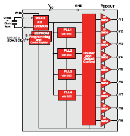
LMK04800 – Ultra High Performance Dual-PLL Jitter Cleaner
 |
|
Parameter
|
LMK04800 Family - Ultra Low Noise Clock Jitter Cleaner with Dual Loop PLLs
|
| Clock Frequencies |
Upto 2.6 Mhz
|
RMS Jitter (156.25 MHz), 1.875MHz to 20 MHz
RMS Jitter (245.76 MHz), 100 Hz to 20 MHz |
57 fs rms
123 fs rms |
|
Number of inputs
|
2x SE or DE.
|
|
Reference Frequency |
SE or DE: 1 MHz to 500 MHz. Includes 25 MHz, 26.5625 MHz, 24.8832 MHz, 100 MHz, 125 MHz, 156.25 MHz.�Crystal: 6 to 20.5 MHz. Includes 12.5 MHz, 15.36 MHz, 19.2 MHz, 19.44 MHz, 20 MHz, and 20.48 MHz
|
| Output Frequency |
LMK04803: 1.8 MHz to 1011.5 MHz 1840 to 2023 MHz with reduced swing/features.�LMK04805: 2.1 MHz to 1185 MHz 2148 to 2370 MHz with reduced swing/features.�LMK04806: 2.3 MHz to 1300 MHz 2370 to 2600 MHz with reduced swing/features.�LMK04808: 2.7 MHz to 1536 MHz 2750 to 3072 MHz with reduced swing/features.
Includes 62.5 MHz, 74.25 MHz, 75 MHz, 100 MHz, 106.2 MHz, 122.88 MHz, 125 MHz, 150 MHz, 155.52 MHz, 156.25 MHz, 200 MHz, 212.5 MHz, 245.76 MHz, 250 MHz, 311.04 MHz, 312.5 MHz, 368.64 MHz, 491.52 MHz, 622.08 MHz, 625 MHz, 737.28 MHz, 983.04 MHz, 1474.56 MHz, 1966.08 MHz
|
| Outputs |
12x LVPECL/LVDS/LVCMOS driven by VCO. 1x LVPECL + 1x LVPECL/LVDS/LVCMOS buffered copy of reference.
|
| Other features |
Analog Delay, Digital Delay, Dynamic Digital Delay, 0-Delay, Holdover, Hitless Switching.
|
|
|
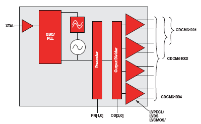
CDCM6100x – Ultra-low jitter (500fs RMS typ, 10kHz – 20MHz) clock generation up to 683MHz. Provides 1, 2, or 4 outputs of LVPECL, LVDS or LVCMOS clocks with an easy-to-use pin-configurable interface. Integrated high performance VCO. Can be used to replace up to 4 low-jitter XOs in a single device. Available in a small footprint 5x5 QFN package.
 |
| Parameter |
CDCM6100x – Pin Programmable Clock Generator Family
|
|
RMS Jitter ( 156.25 MHz),
1.875MHz – 20 MHz
|
152 fs, rms
|
|
Reference Frequency
|
Includes 25MHz, 26.5625MHz, 24.8832MHz
|
|
Number of inputs
|
1x SE or crystal
|
|
Output Frequency
|
44 MHz – 683 MHz
Includes 62.5MHz, 74.25MHz, 75MHz, 100 MHz, 106.2MHz, 125 MHz, 150MHz, 155.52 MHz, 156.25 MHz, 200 MHz, 212.5 MHz, 250 MHz, 311.04 MHz, 312.5 MHz, 622.08MHz, 625MHz
|
|
Outputs
|
4xLVPECL/LVDS or 8xLVCMOS, 1xLVCMOS Bypass
|
|
|
CDCE(L)9xx – Family of modular PLL-based programmable clock synthesizers. Generates up to 9 LVCMOS clocks from a single input frequency, either LVCMOS or XTAL input. Each output can be programmed for any clock frequency up to 230MHz, using up to four independent configurable fractional PLLs. Deep M/N divider ratio allows for the generation of 0-ppm clocks. All PLLs support spreadspectrum clocking (SSC). Onboard EEPROM for easy customization of device over I2C interface. Small footprint TSSOP package help to reduce board space requirements.
|
|
Parameter
|
CDCE9xx – Programmable 1/2/3/4 PLL Clock Generator Family
|
|
Reference Frequency
|
8 – 32 MHz (Crystal), Upto 160 MHz (Single Ended)
|
|
Number of inputs
|
1x SE or crystal
|
|
Output Frequency
|
Upto 230 MHz
|
|
Outputs
|
1, 3, 7, 9 Single Ended Clocks
|
|
Special Features
|
Fractional PLL, Spread Spectrum Clocking, Crystal Buffer
|
|
Clock Distribution
|
CDCLVD12xx/21xx – Family of industry's lowest additive jitter LVDS clock distribution buffers. Up to 16 low additive jitter (<300fs RMS typ, 10kHz – 20MHz), low skew clock outputs. Universal input support for LVPECL, LVDS or LVCMOS clocks. Signaling rate up to 800MHz. Small footprint QFN package help to reduce board space requirements.
|
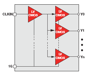
CDCLVC11xx – Family of industry's lowest additive jitter LVCMOS clock distribution buffers. Up to 12 low additive jitter (<100fs RMS tip, 10kHz – 20MHz), low skew clock outputs. Signaling rate up to 250MHz. Small footprint TSSOP package help to reduce board space requirements.
 |
|
Parameters
|
CDCLVC11xx
|
CDCLVD12xx
|
CDCLVP12xx
|
|
Input
|
Upto 250 MHz. LVCMOS
|
Upto 800 MHz. LVPECL, LVDS, LVCMOS/TTL
|
Upto 2 Ghz.
LVPECL, LVDS, LVCMOS/TTL
|
|
Output
|
LVCMOS
|
LVDS
|
LVPECL
|
|
Number of Outputs
|
Family supports 02/03/04/06/08/10/12 outputs
|
Family supports 04/08/12/16 outputs
|
Family supports 04/08/12/16 outputs
|
|
Additive Jitter (RMS)
|
< 100 fs
|
< 300 fs
|
< 100 fs
|
|
Skew
|
15 ps
|
15 ps (1204),
50 ps (1216)
|
15 ps (1204),
30 ps (1216)
|
|
Special features
|
Small Package, Ultra low jitter & skew
|
2.5V supply. Ultra low jitter & skew
|
Ultra low Jitter & skew
|
|
Clocking for FPGA's
 |
|