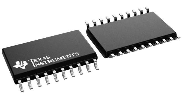
封装信息
| 封装 | 引脚 SOIC (DW) | 20 |
| 工作温度范围 (°C) -40 to 125 |
| 包装数量 | 包装 25 | TUBE |
SN74LVC541A 的特性
- Operate From 1.65 V to 3.6 V
- Inputs Accept Voltages to 5.5 V
- Max tpd of 5.1 ns at 3.3 V
- Typical VOLP (Output Ground Bounce)
<0.8 V at VCC = 3.3 V, TA = 25°C - Typical VOHV (Output VOH Undershoot)
>2 V at VCC = 3.3 V, TA = 25°C - Support Mixed-Mode Signal Operation on
All Ports (5-V Input/Output Voltage With
3.3-V VCC) - Ioff Supports Partial-Power-Down Mode Operation
- Latch-Up Performance Exceeds 250 mA
Per JESD 17 - ESD Protection Exceeds JESD 22
- 2000-V Human-Body Model (A114-A)
- 200-V Machine Model (A115-A)
- 1000-V Charged-Device Model (C101)
- On Products Compliant to MIL-PRF-38535,
All Parameters Are Tested Unless Otherwise Noted.
On All Other Products, Production Processing Does
Not Necessarily Include Testing of All Parameters.
SN74LVC541A 的说明
The SN54LVC541A octal buffer/driver is designed for 2.7-V to 3.6-V VCC operation, and the SN74LVC541A octal buffer/driver is designed for 1.65-V to 3.6-V VCC operation.
The ’LVC541A devices are ideal for driving bus lines or buffering memory address registers.
These devices feature inputs and outputs on opposite sides of the package to facilitate printed circuit board layout.
The 3-state control gate is a 2-input AND gate with active-low inputs so that, if either output enable (OE1 or OE2) input is high, all eight outputs are in the high-impedance state.
Inputs can be driven from either 3.3-V or 5-V devices. This feature allows the use of these devices as translators in a mixed 3.3-V/5-V system environment.
These devices are fully specified for partial-power-down applications using Ioff. The Ioff circuitry disables the outputs, preventing damaging current backflow through the devices when they are powered down.
To ensure the high-impedance state during power up or power down, OE should be tied to VCC through a pullup resistor; the minimum value of the resistor is determined by the current-sinking capability of the driver.
