封装信息
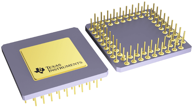
| 封装 | 引脚 CPGA (GB) | 68 |
| 工作温度范围 (°C) -55 to 125 |
| 包装数量 | 包装 21 | JEDEC TRAY (5+1) |
SN54ACT8990 的特性
- Members of the Texas Instruments SCOPETM Family of Testability Products
- Compatible With the IEEE Standard 1149.1-1990 (JTAG) Test Access Port and Boundary-Scan Architecture
- Control Operation of Up to Six Parallel Target Scan Paths
- Accommodate Pipeline Delay to Target of Up to 31 Clock Cycles
- Scan Data Up to 232 Clock Cycles
- Execute Instructions for Up to 232 Clock Cycles
- Each Device Includes Four Bidirectional Event Pins for Additional Test Capability
- Inputs Are TTL-Voltage Compatible
- EPICTM (Enhanced-Performance Implanted CMOS) 1-
 m Process
- Packaged in 44-Pin Plastic Leaded Chip Carrier (FN), 68-Pin
Ceramic Pin Grid Array (GB), and 68-Pin Ceramic Quad Flat Packages
(HV)
SCOPE and EPIC are trademarks of Texas Instruments Incorporated.
SN54ACT8990 的说明
The 'ACT8990 test-bus controllers (TBC) are members of the Texas Instruments SCOPETM testability integrated-circuit family. This family of components supports IEEE Standard 1149.1-1990 (JTAG) boundary scan to facilitate testing of complex circuit-board assemblies. The 'ACT8990 differ from other SCOPETM integrated circuits. Their function is to control the JTAG serial-test bus rather than being target boundary-scannable devices.
The required signals of the JTAG serial-test bus - test clock (TCK), test mode select (TMS), test data input (TDI), and test data output (TDO) can be connected from the TBC to a target device without additional logic. This is done as a chain of IEEE Standard 1149.1-1990 boundary-scannable components that share the same serial-test bus. The TBC generates TMS and TDI signals for its target(s), receives TDO signals from its target(s), and buffers its test clock input (TCKI) to a test clock output (TCKO) for distribution to its target(s). The TMS, TDI, and TDO signals can be connected to a target directly or via a pipeline, with a retiming delay of up to 31 bits. Since the TBC can be configured to generate up to six separate TMS signals [TMS (5-0)], it can be used to control up to six target scan paths that are connected in parallel (i.e., sharing common TCK, TDI, and TDO signals).
While most operations of the TBC are synchronous to TCKI, a test-off (TOFF\) input is provided for output control of the target interface, and a test-reset (TRST\) input is provided for hardware/software reset of the TBC. In addition, four event [EVENT (3-0)] I/Os are provided for asynchronous communication to target device(s). Each event has its own event generation/detection logic, and detected events can be counted by two 16-bit counters.
The TBC operates under the control of a host microprocessor/microcontroller via the 5-bit address bus [ADRS (4-0)] and the 16-bit read/write data bus [DATA (15-0)]. Read (RD\) and write (WR\) strobes are implemented such that the critical host-interface timing is independent of the TCKI period. Any one of 24 registers can be addressed for read and/or write operations. In addition to control and status registers, the TBC contains two command registers, a read buffer, and a write buffer. Status of the TBC is transmitted to the host via ready (RDY\) and interrupt (INT\) outputs.
Major commands can be issued by the host to cause the TBC to generate the TMS sequences necessary to move the target(s) from any stable test-access-port (TAP) controller state to any other stable TAP state, to execute instructions in the Run-Test/Idle TAP state, or to scan instruction or test data through the target(s). A 32-bit counter can be preset to allow a predetermined number of execution or scan operations.
Serial data that appears at the selected TDI input (TDI1 or TDI0) is transferred into the read buffer, which can be read by the host to obtain up to 16 bits of the serial-data stream. Serial data that is transmitted from the TDO output is written by the host to the write buffer.
The SN54ACT8990 is characterized for operation over the full military temperature range of -55°C to 125°C. The SN74ACT8990 is characterized for operation from 0°C to 70°C.
NC - No internal connection