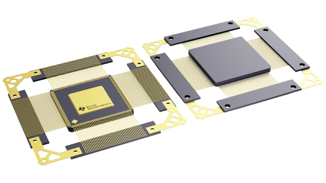
封装信息
| 封装 | 引脚 CFP (HFG) | 164 |
| 工作温度范围 (°C) -55 to 125 |
| 包装数量 | 包装 10 | JEDEC TRAY (5+1) |
SMJ320VC33 的特性
- High-Performance Floating-Point Digital Signal
Processor (DSP)- SMx320VC33-150
- 13-ns Instruction Cycle Time
- 150 Million Floating-Point Operations per
Second (MFLOPS) - 75 Million Instructions per Second (MIPS)
- SMx320VC33-150
- 34K × 32-Bit (1.1-Mbit) On-Chip Words of Dual-
Access Static Random-Access Memory (SRAM)
Configured in 2 × 16K plus 2 × 1K Blocks to
Improve Internal Performance - x5 Phase-Locked Loop (PLL) Clock Generator
- Very-Low Power: <200 mW at 150 MFLOPS
- 32-Bit High-Performance CPU
- 16-/32-Bit Integer and 32-/40-Bit Floating-Point
Operations - Four Internally Decoded Page Strobes to Simplify
Interface to I/O and Memory Devices - Boot-Program Loader
- EDGEMODE Selectable External Interrupts
- 32-Bit Instruction Word, 24-Bit Addresses
- Eight Extended-Precision Registers
- Fabricated Using the 0.18-µm (leff – Effective Gate
Length) TImeline™ Technology by Texas
Instruments - On-Chip Scan-Based Emulation Logic, IEEE Std
1149.1 (JTAG) - On-Chip Memory-Mapped Peripherals:
- One Serial Port
- Two 32-Bit Timers
- Direct Memory Access (DMA) Coprocessor for
Concurrent I/O and CPU Operation
- 164-Pin Low-Profile Quad Flatpack (HFG Suffix)
- 144-Pin Non-Hermetic Ceramic Ball Grid Array
(CBGA) (GNM Suffix) - Two Address Generators With Eight Auxiliary
Registers and Two Auxiliary Register Arithmetic
Units (ARAUs) - Two Low-Power Modes
- Two- and Three-Operand Instructions
- Parallel Arithmetic/Logic Unit (ALU) and Multiplier
Execution in a Single Cycle - Block-Repeat Capability
- Zero-Overhead Loops With Single-Cycle
Branches - Conditional Calls and Returns
- Interlocked Instructions for Multiprocessing
Support - Bus-Control Registers Configure Strobe-Control
Wait-State Generation - 1.8-V (Core) and 3.3-V (I/O) Supply Voltages
All trademarks are the property of their respective owners.
SMJ320VC33 的说明
The SMx320VC33 DSP is a 32-bit, floating-point processor manufactured in 0.18-µm four-level-metal CMOS (TImeline) technology. The SMx320VC33 is part of the SM320C3x™ generation of DSPs from Texas Instruments.
The SM320C3x internal busing and special digital-signal-processing instruction set have the speed and flexibility to execute up to 150 MFLOPS. The SMx320VC33 optimizes speed by implementing functions in hardware that other processors implement through software or microcode. This hardware-intensive approach provides performance previously unavailable on a single chip.
The SMx320VC33 can perform parallel multiply and ALU operations on integer or floating-point data in a single cycle. Each processor also possesses a general-purpose register file, a program cache, dedicated ARAUs, internal dual-access memories, one DMA channel supporting concurrent I/O, and a short machine-cycle time. These features result in high performance and ease of use. General-purpose applications are greatly enhanced by the large address space, multiprocessor interface, internally and externally generated wait states, one external interface port, two timers, one serial port, and multiple-interrupt structure.
The SM320C3x supports a wide variety of system applications from host processor to dedicated coprocessor. High-level-language support is easily implemented through a register-based architecture, large address space, powerful addressing modes, flexible instruction set, and well-supported floating-point arithmetic.
The SM/SMJ320VC33 is a superset of the TMS320C31. Designers now have an additional 1Mb of on-chip SRAM, a maximum throughput of 150 MFLOPS, and several I/O enhancements that allow easy upgrades to current systems or creation of new baselines. This data sheet provides information required to fully use the new features of the SM/SMJ320VC33 device. For general TMS320C3x architecture and programming information, see the TMS320C3x User’s Guide (SPRU031).
The SMx320VC33 device is packaged in 164-pin low-profile quad flatpacks (HFG suffix) and in 144-ball fine pitch ball grid arrays (GNL and GNM suffix).
