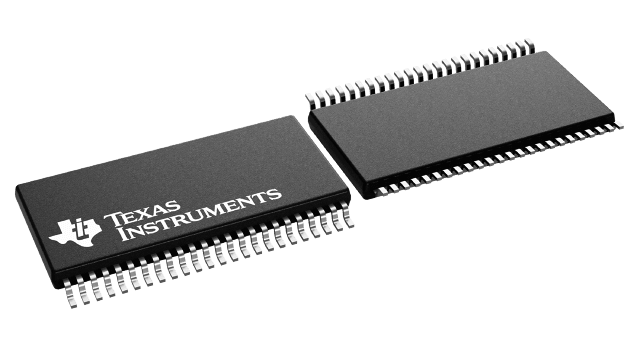
封装信息
| 封装 | 引脚 TSSOP (DGG) | 48 |
| 工作温度范围 (°C) -10 to 70 |
| 包装数量 | 包装 1,000 | LARGE T&R |
DS90CF363B 的特性
- No Special Start-up Sequence Required between Clock/Data and /PD Pins. Input Signal (Clock and Data) can be Applied Either Before or After the Device is Powered.
- Support Spread Spectrum Clocking up to 100KHz Frequency Modulation & Deviations of ±2.5% Center Spread or −5% Down Spread.
- "Input Clock Detection" Feature will Pull all LVDS Pairs to Logic Low when Input Clock is Missing and when /PD Pin is Logic High.
- 18 to 68 MHz Shift Clock Support
- Best–in–Class Set & Hold Times on TxINPUTs
- Tx Power Consumption < 130 mW (typ) @65MHz Grayscale
- 40% Less Power Dissipation than BiCMOS Alternatives
- Tx Power-Down Mode < 37μW (typ)
- Supports VGA, SVGA, XGA and Dual Pixel SXGA.
- Narrow Bus Reduces Cable Size and Cost
- Up to 1.3 Gbps Throughput
- Up to 170 Megabytes/sec Bandwidth
- 345 mV (typ) Swing LVDS Devices for Low EMI
- PLL Requires no External Components
- Compatible with TIA/EIA-644 LVDS Standard
- Low Profile 48-lead TSSOP Package
- Improved Replacement for:
- SN75LVDS84, DS90CF363A
All trademarks are the property of their respective owners.
DS90CF363B 的说明
The DS90CF363B transmitter converts 21 bits of CMOS/TTL data into three LVDS (Low Voltage Differential Signaling) data streams. A phase-locked transmit clock is transmitted in parallel with the data streams over a fourth LVDS link. Every cycle of the transmit clock 21 bits of input data are sampled and transmitted. At a transmit clock frequency of 65 MHz, 18 bits of RGB data and 3 bits of LCD timing and control data (FPLINE, FPFRAME, DRDY) are transmitted at a rate of 455 Mbps per LVDS data channel. Using a 65 MHz clock, the data throughput is 170 Mbytes/sec. The DS90CF363B is fixed as a Falling edge strobe transmitter and will interoperate with a Falling edge strobe Receiver (DS90CF366) without any translation logic.
This chipset is an ideal means to solve EMI and cable size problems associated with wide, high speed TTL interfaces.
