SGLS155B February 2003 – November 2016 TPS768-Q1
PRODUCTION DATA.
- 1 Features
- 2 Applications
- 3 Description
- 4 Revision History
- 5 Pin Configuration and Functions
- 6 Specifications
- 7 Parameter Measurement Information
- 8 Detailed Description
- 9 Application and Implementation
- 10Power Supply Recommendations
- 11Layout
- 12Device and Documentation Support
- 13Mechanical, Packaging, and Orderable Information
1 Features
- Qualified for Automotive Applications
- AEC-Q100 Qualified With the Following Results:
- Device Temperature Grade 1: –40°C to 125°C Ambient Operating Temperature Range
- Device HBM ESD Classification Level H2
- Device CDM ESD Classification Level C4B
- 1-A Low-Dropout (LDO) Voltage Regulator
- Available in 1.8-V, 2.5-V, 3.3-V, and 5-V Fixed-Output and an Adjustable Version
- Dropout Voltage Down to 230 mV at 1 A (TPS76850-Q1)
- Ultralow 85-μA Typical Quiescent Current
- Fast Transient Response
- 2% Tolerance Over Specified Conditions for Fixed-Output Versions
- Open-Drain Power Good (See TPS767xx-Q1 for Power-On Reset With 200-ms Delay Option)
- 20-Pin TSSOP (PWP) Package
- Thermal Shutdown Protection
2 Applications
- Automotive
- Power Train
- Cluster
- ADAS
3 Description
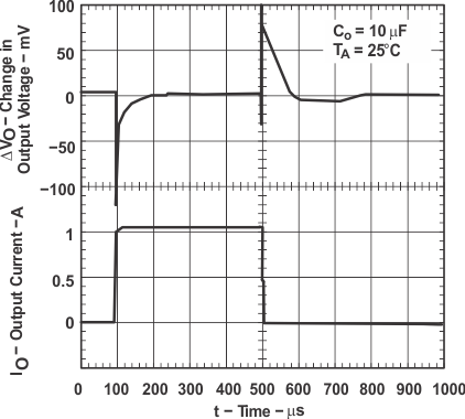
This device is designed to have a fast transient response and be stable with 10 μF capacitors. This combination provides high performance at a reasonable cost.
Because the PMOS device behaves as a low-value resistor, the dropout voltage is very low (typically 230 mV at an output current of 1 A for the TPS76850-Q1) and is directly proportional to the output current. Additionally, because the PMOS pass element is a voltage-driven device, the quiescent current is very low and independent of output loading (typically 85 μA over the full range of output current, 0 mA to 1 A). These two key specifications yield a significant improvement in operating life for battery-powered systems. This LDO family also features a shutdown mode; applying a TTL high signal to the enable (EN) input shuts down the regulator, reducing the quiescent current to less than 1 μA at TJ = 25°C.
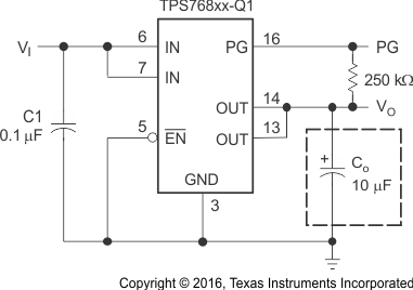
Power good (PG) is an active-high output, which can be used to implement a power-on reset or a low-battery indicator.
The TPS768xx-Q1 is offered in 1.8-V, 2.5-V, 3.3-V, and 5-V fixed-voltage versions and in an adjustable version (programmable over the range of 1.2 V to 5.5 V). Output voltage tolerance is specified as a maximum of 2% over line, load, and temperature ranges. The TPS768xx-Q1 family is available in a 20-pin PWP package.
Device Information(1)
| PART NUMBER | PACKAGE | BODY SIZE (NOM) |
|---|---|---|
| TPS768xx-Q1 | HTSSOP (20) | 6.50 mm × 4.40 mm |
- For all available packages, see the orderable addendum at the end of the data sheet.

