SPRS563G September 2008 – June 2014 OMAP-L137
PRODUCTION DATA.
- 1 OMAP-L137 Low-Power Applications Processor
- 2Revision History
-
3Device Overview
- 3.1 Device Characteristics
- 3.2 Device Compatibility
- 3.3 ARM Subsystem
- 3.4 DSP Subsystem
- 3.5 Memory Map Summary
- 3.6 Pin Assignments
- 3.7
Terminal Functions
- 3.7.1 Device Reset and JTAG
- 3.7.2 High-Frequency Oscillator and PLL
- 3.7.3 Real-Time Clock and 32-kHz Oscillator
- 3.7.4 External Memory Interface A (ASYNC, SDRAM)
- 3.7.5 External Memory Interface B (only SDRAM)
- 3.7.6 Serial Peripheral Interface Modules (SPI0, SPI1)
- 3.7.7 Enhanced Capture/Auxiliary PWM Modules (eCAP0, eCAP1, eCAP2)
- 3.7.8 Enhanced Pulse Width Modulators (eHRPWM0, eHRPWM1, eHRPWM2)
- 3.7.9 Enhanced Quadrature Encoder Pulse Module (eQEP)
- 3.7.10 Boot
- 3.7.11 Universal Asynchronous Receiver/Transmitters (UART0, UART1, UART2)
- 3.7.12 Inter-Integrated Circuit Modules(I2C0, I2C1)
- 3.7.13 Timers
- 3.7.14 Universal Host-Port Interface (UHPI)
- 3.7.15 Multichannel Audio Serial Ports (McASP0, McASP1, McASP2)
- 3.7.16 Universal Serial Bus Modules (USB0, USB1)
- 3.7.17 Ethernet Media Access Controller (EMAC)
- 3.7.18 Multimedia Card/Secure Digital (MMC/SD)
- 3.7.19 Liquid Crystal Display Controller (LCD)
- 3.7.20 Reserved and No Connect
- 3.7.21 Supply and Ground
- 3.7.22 Unused USB0 (USB2.0) and USB1 (USB1.1) Pin Configurations
-
4Device Configuration
- 4.1 Boot Modes
- 4.2 SYSCFG Module
- 4.3 Pullup/Pulldown Resistors
- 4.4 Absolute Maximum Ratings Over Operating Case Temperature Range (Unless Otherwise Noted)
- 4.5 Handling Ratings
- 4.6 Recommended Operating Conditions
- 4.7 Notes on Recommended Power-On Hours (POH)
- 4.8 Electrical Characteristics Over Recommended Ranges of Supply Voltage and Operating Case Temperature (Unless Otherwise Noted)
-
5Peripheral Information and Electrical Specifications
- 5.1 Parameter Information
- 5.2 Recommended Clock and Control Signal Transition Behavior
- 5.3 Power Supplies
- 5.4 Reset
- 5.5 Crystal Oscillator or External Clock Input
- 5.6 Clock PLLs
- 5.7 Interrupts
- 5.8 General-Purpose Input/Output (GPIO)
- 5.9 EDMA
- 5.10 External Memory Interface A (EMIFA)
- 5.11 External Memory Interface B (EMIFB)
- 5.12 Memory Protection Units
- 5.13 MMC / SD / SDIO (MMCSD)
- 5.14 Ethernet Media Access Controller (EMAC)
- 5.15 Management Data Input/Output (MDIO)
- 5.16 Multichannel Audio Serial Ports (McASP0, McASP1, and McASP2)
- 5.17 Serial Peripheral Interface Ports (SPI0, SPI1)
- 5.18 Enhanced Capture (eCAP) Peripheral
- 5.19 Enhanced Quadrature Encoder (eQEP) Peripheral
- 5.20 Enhanced High-Resolution Pulse-Width Modulator (eHRPWM)
- 5.21 LCD Controller
- 5.22 Timers
- 5.23 Inter-Integrated Circuit Serial Ports (I2C0, I2C1)
- 5.24 Universal Asynchronous Receiver/Transmitter (UART)
- 5.25 USB1 Host Controller Registers (USB1.1 OHCI)
- 5.26 USB0 OTG (USB2.0 OTG)
- 5.27 Host-Port Interface (UHPI)
- 5.28 Power and Sleep Controller (PSC)
- 5.29 Programmable Real-Time Unit Subsystem (PRUSS)
- 5.30 Emulation Logic
- 5.31 IEEE 1149.1 JTAG
- 5.32 Real Time Clock (RTC)
- 6Device and Documentation Support
- 7Mechanical Packaging and Orderable Information
1 OMAP-L137 Low-Power Applications Processor
1.1 Features
- Software Support
- TI DSP/BIOS™
- Chip Support Library and DSP Library
- Dual Core SoC
- 375- and 456-MHz ARM926EJ-S™ RISC MPU
- 375- and 456-MHz C674x VLIW DSP
- ARM926EJ-S Core
- 32-Bit and 16-Bit (Thumb®) Instructions
- DSP Instruction Extensions
- Single Cycle MAC
- ARM® Jazelle® Technology
- Embedded ICE-RT™ for Real-Time Debug
- ARM9™ Memory Architecture
- 16KB of Instruction Cache
- 16KB of Data Cache
- 8KB of RAM (Vector Table)
- 64KB of ROM
- C674x Instruction Set Features
- Superset of the C67x+ and C64x+ ISAs
- Up to 3648 MIPS and 2736 MFLOPS C674x
- Byte-Addressable (8-, 16-, 32-, and 64-Bit Data)
- 8-Bit Overflow Protection
- Bit-Field Extract, Set, Clear
- Normalization, Saturation, Bit-Counting
- Compact 16-Bit Instructions
- C674x Two-Level Cache Memory Architecture
- 32KB of L1P Program RAM/Cache
- 32KB of L1D Data RAM/Cache
- 256KB of L2 Unified Mapped RAM/Cache
- Flexible RAM/Cache Partition (L1 and L2)
- Enhanced Direct Memory Access Controller 3 (EDMA3):
- 2 Transfer Controllers
- 32 Independent DMA Channels
- 8 Quick DMA Channels
- Programmable Transfer Burst Size
- TMS320C674x Fixed- and Floating-Point VLIW DSP Core
- Load-Store Architecture with Nonaligned Support
- 64 General-Purpose Registers (32-Bit)
- Six ALU (32- and 40-Bit) Functional Units
- Supports 32-Bit Integer, SP (IEEE Single Precision/32-Bit) and DP (IEEE Double Precision/64-Bit) Floating Point
- Supports up to Four SP Additions Per Clock, Four DP Additions Every 2 Clocks
- Supports up to Two Floating-Point (SP or DP) Reciprocal Approximation (RCPxP) and Square-Root Reciprocal Approximation (RSQRxP) Operations Per Cycle
- Two Multiply Functional Units
- Mixed-Precision IEEE Floating Point Multiply Supported up to:
- 2 SP x SP -> SP Per Clock
- 2 SP x SP -> DP Every Two Clocks
- 2 SP x DP -> DP Every Three Clocks
- 2 DP x DP -> DP Every Four Clocks
- Fixed-Point Multiply Supports Two 32 x 32-Bit Multiplies, Four 16 x 16-Bit Multiplies, or Eight 8 x 8-Bit Multiplies per Clock Cycle, and Complex Multiples
- Mixed-Precision IEEE Floating Point Multiply Supported up to:
- Instruction Packing Reduces Code Size
- All Instructions Conditional
- Hardware Support for Modulo Loop
Operation - Protected Mode Operation
- Exceptions Support for Error Detection and Program Redirection
- 128KB of RAM Shared Memory
- 3.3-V LVCMOS I/Os (Except for USB Interfaces)
- Two External Memory Interfaces:
- EMIFA
- NOR (8- or 16-Bit-Wide Data)
- NAND (8- or 16-Bit-Wide Data)
- 16-Bit SDRAM with 128-MB Address Space
- EMIFB
- 32-Bit or 16-Bit SDRAM with 256-MB Address Space
- EMIFA
- Three Configurable 16550-Type UART Modules:
- UART0 with Modem Control Signals
- Autoflow Control Signals (CTS, RTS) on UART0 Only
- 16-Byte FIFO
- 16x or 13x Oversampling Option
- LCD Controller
- Two Serial Peripheral Interfaces (SPIs) Each with One Chip Select
- Multimedia Card (MMC)/Secure Digital (SD) Card Interface with Secure Data I/O (SDIO)
- Two Master and Slave Inter-Integrated Circuit (I2C Bus™)
- One Host-Port Interface (HPI) with 16-Bit-Wide Muxed Address/Data Bus for High Bandwidth
- Programmable Real-Time Unit Subsystem (PRUSS)
- Two Independent Programmable Realtime Unit (PRU) Cores
- 32-Bit Load and Store RISC Architecture
- 4KB of Instruction RAM per Core
- 512 Bytes of Data RAM per Core
- PRUSS can be Disabled via Software to Save Power
- Standard Power-Management Mechanism
- Clock Gating
- Entire Subsystem Under a Single PSC Clock Gating Domain
- Dedicated Interrupt Controller
- Dedicated Switched Central Resource
- Two Independent Programmable Realtime Unit (PRU) Cores
- USB 1.1 OHCI (Host) with Integrated PHY (USB1)
- USB 2.0 OTG Port with Integrated PHY (USB0)
- USB 2.0 High- and Full-Speed Client
- USB 2.0 High-, Full-, and Low-Speed Host
- End Point 0 (Control)
- End Points 1,2,3,4 (Control, Bulk, Interrupt or ISOC) RX and TX
- Three Multichannel Audio Serial Ports (McASPs):
- Six Clock Zones and 28 Serial Data Pins
- Supports TDM, I2S, and Similar Formats
- DIT-Capable (McASP2)
- FIFO Buffers for Transmit and Receive
- 10/100 Mbps Ethernet MAC (EMAC):
- IEEE 802.3 Compliant (3.3-V I/O Only)
- RMII Media-Independent Interface
- Management Data I/O (MDIO) Module
- Real-Time Clock with 32-kHz Oscillator and Separate Power Rail
- One 64-Bit General-Purpose Timer (Configurable as Two 32-Bit Timers)
- One 64-Bit General-Purpose Watchdog Timer (Configurable as Two 32-Bit General-Purpose Timers)
- Three Enhanced Pulse Width Modulators (eHRPWMs):
- Dedicated 16-Bit Time-Base Counter with Period and Frequency Control
- 6 Single Edge, 6 Dual Edge Symmetric, or 3 Dual Edge Asymmetric Outputs
- Dead-Band Generation
- PWM Chopping by High-Frequency Carrier
- Trip Zone Input
- Three 32-Bit Enhanced Capture (eCAP) Modules:
- Configurable as 3 Capture Inputs or 3 Auxiliary Pulse Width Modulator (APWM) Outputs
- Single-Shot Capture of up to Four Event Time-Stamps
- Two 32-Bit Enhanced Quadrature Encoder Pulse (eQEP) Modules
- 256-Ball Pb-Free Plastic Ball Grid Array (PBGA) [ZKB Suffix], 1.0-mm Ball Pitch
- Commercial, Industrial, Extended, or Automotive Temperature
1.2 Applications
- A/V Receivers
- Automotive Amplifiers
- Soundbars
- Home Theatre Systems
- Professional Audio
- Network Streaming Audio
1.3 Description
The OMAP-L137 device is a low-power applications processor based on an ARM926EJ-S and a TMS320C674x DSP core. It consumes significantly lower power than other members of the TMS320C6000™ platform of DSPs.
The OMAP-L137 device enables original-equipment manufacturers (OEMs) and original-design manufacturers (ODMs) to quickly bring to market devices featuring robust operating systems support, rich user interfaces, and high processing performance life through the maximum flexibility of a fully integrated mixed processor solution.
The dual-core architecture of the OMAP-L137 device provides benefits of both DSP and Reduced Instruction Set Computer (RISC) technologies, incorporating a high-performance TMS320C674x DSP core and an ARM926EJ-S core.
The ARM926EJ-S is a 32-bit RISC processor core that performs 32-bit or 16-bit instructions and processes 32-bit, 16-bit, or 8-bit data. The core uses pipelining so that all parts of the processor and memory system can operate continuously.
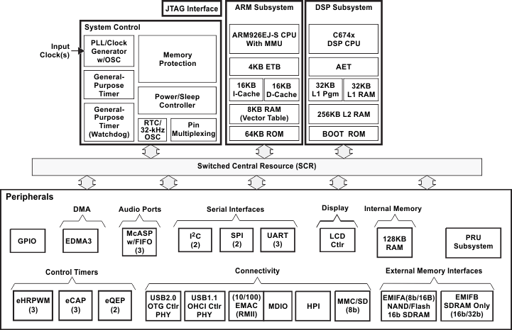
The ARM core has a coprocessor 15 (CP15), protection module, and data and program Memory Management Units (MMUs) with table look-aside buffers. The ARM core has separate 16-KB instruction and 16KB of data caches. Both memory blocks are four-way associative with virtual index virtual tag (VIVT). The ARM core also has 8KB of RAM (Vector Table) and 64KB of ROM.
The OMAP-L137 DSP core uses a two-level cache-based architecture. The Level 1 program cache (L1P) is a 32-KB direct mapped cache and the Level 1 data cache (L1D) is a 32-KB 2-way set-associative cache. The Level 2 program cache (L2P) consists of a 256-KB memory space that is shared between program and data space. L2 memory can be configured as mapped memory, cache, or combinations of the two. Although the DSP L2 is accessible by ARM and other hosts in the system, an additional 128KB of RAM shared memory is available for use by other hosts without affecting DSP performance.
The peripheral set includes: a 10/100 Mbps Ethernet MAC (EMAC) with a management data input/output (MDIO) module; two I2C Bus interfaces; 3 multichannel audio serial ports (McASPs) with 16/12/4 serializers and FIFO buffers; two 64-bit general-purpose timers each configurable (one configurable as watchdog); a configurable 16-bit host-port interface (HPI); up to 8 banks of 16 pins of general-purpose input/output (GPIO) with programmable interrupt/event generation modes, multiplexed with other peripherals; 3 UART interfaces (one with both RTS and CTS); three enhanced high-resolution pulse width modulator (eHRPWM) peripherals; three 32-bit enhanced capture (eCAP) module peripherals which can be configured as 3 capture inputs or 3 auxiliary pulse width modulator (APWM) outputs; two 32-bit enhanced quadrature encoded pulse (eQEP) peripherals; and 2 external memory interfaces: an asynchronous and SDRAM external memory interface (EMIFA) for slower memories or peripherals, and a higher speed memory interface (EMIFB) for SDRAM.
The Ethernet Media Access Controller (EMAC) provides an efficient interface between the OMAP-L137 device and the network. The EMAC supports both 10Base-T and 100Base-TX, or 10 Mbps and 100 Mbps in either half- or full-duplex mode. Additionally, an MDIO interface is available for PHY configuration.
The HPI, I2C, SPI, USB1.1, and USB2.0 ports allow the OMAP-L137 device to easily control peripheral devices and/or communicate with host processors.
The rich peripheral set provides the ability to control external peripheral devices and communicate with external processors. For details on each of the peripherals, see the related sections later in this document and the associated peripheral reference guides.
The OMAP-L137 device has a complete set of development tools for both the ARM and DSP. These include C compilers, a DSP assembly optimizer to simplify programming and scheduling, and a Windows® debugger interface for visibility into source code execution.
1.4 Functional Block Diagram