ZHCSM31B September   2020  – March 2022 ADC3660

PRODUCTION DATA  

  1. 特性
  2. 应用
  3. 说明
  4. Revision History
  5. Pin Configuration and Functions
  6. Specifications
    1. 6.1 Absolute Maximum Ratings
    2. 6.2 ESD Ratings
    3. 6.3 Recommended Operating Conditions
    4. 6.4 Thermal Information
    5. 6.5 Electrical Characteristics - Power Consumption
    6. 6.6 Electrical Characteristics - DC Specifications
    7. 6.7 Electrical Characteristics - AC Specifications
    8. 6.8 Timing Requirements
    9. 6.9 Typical Characteristics
  7. Parameter Measurement Information
  8. Detailed Description
    1. 8.1 Overview
    2. 8.2 Functional Block Diagram
    3. 8.3 Feature Description
      1. 8.3.1 Analog Input
        1. 8.3.1.1 Analog Input Bandwidth
        2. 8.3.1.2 Analog Front End Design
          1. 8.3.1.2.1 Sampling Glitch Filter Design
          2. 8.3.1.2.2 Analog Input Termination and DC Bias
            1. 8.3.1.2.2.1 AC-Coupling
            2. 8.3.1.2.2.2 DC-Coupling
        3. 8.3.1.3 Auto-Zero Feature
      2. 8.3.2 Clock Input
        1. 8.3.2.1 Single Ended vs Differential Clock Input
        2. 8.3.2.2 Signal Acquisition Time Adjust
      3. 8.3.3 Voltage Reference
        1. 8.3.3.1 Internal voltage reference
        2. 8.3.3.2 External voltage reference (VREF)
        3. 8.3.3.3 External voltage reference with internal buffer (REFBUF)
      4. 8.3.4 Digital Down Converter
        1. 8.3.4.1 DDC MUX
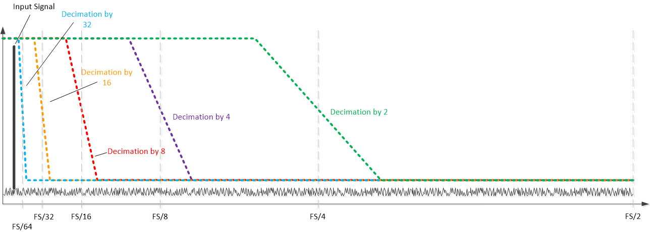
        2. 8.3.4.2 Digital Filter Operation
          1. 8.3.4.2.1 FS/4 Mixing with Real Output
        3. 8.3.4.3 Numerically Controlled Oscillator (NCO) and Digital Mixer
        4. 8.3.4.4 Decimation Filter
        5. 8.3.4.5 SYNC
        6. 8.3.4.6 Output Formatting with Decimation
      5. 8.3.5 Digital Interface
        1. 8.3.5.1 SDR Output Clocking
        2. 8.3.5.2 Output Data Format
        3. 8.3.5.3 Output Formatter
        4. 8.3.5.4 Output Bit Mapper
        5. 8.3.5.5 Output Interface/Mode Configuration
          1. 8.3.5.5.1 Configuration Example
      6. 8.3.6 Test Pattern
    4. 8.4 Device Functional Modes
      1. 8.4.1 Normal Operation
      2. 8.4.2 Power Down Options
      3. 8.4.3 Digital Channel Averaging
    5. 8.5 Programming
      1. 8.5.1 Configuration using PINs only
      2. 8.5.2 Configuration using the SPI interface
        1. 8.5.2.1 Register Write
        2. 8.5.2.2 Register Read
    6. 8.6 Register Maps
      1. 8.6.1 Detailed Register Description
  9. Application and Implementation
    1. 9.1 Typical Application
      1. 9.1.1 Design Requirements
      2. 9.1.2 Detailed Design Procedure
        1. 9.1.2.1 Input Signal Path
        2. 9.1.2.2 Sampling Clock
        3. 9.1.2.3 Voltage Reference
      3. 9.1.3 Application Curves
    2. 9.2 Initialization Set Up
      1. 9.2.1 Register Initialization During Operation
  10. 10Power Supply Recommendations
  11. 11Layout
    1. 11.1 Layout Guidelines
    2. 11.2 Layout Example
  12. 12Device and Documentation Support
    1. 12.1 支持资源
    2. 12.2 Trademarks
    3. 12.3 Electrostatic Discharge Caution
    4. 12.4 术语表
  13. 13Mechanical, Packaging, and Orderable Information

Digital Filter Operation

The complex decimation operation is illustrated with an example in Figure 8-19. First the input signal (and the negative image) are frequency shifted by the NCO frequency as shown on the left. Next a digital filter is applied (centered around 0 Hz) and the output data rate is decimated - in this example the output data rate FS,OUT = FS/8 with a Nyquist zone of FS/16. During the complex mixing the spectrum (signal and noise) is split into real and complex parts and thus the amplitude is reduced by 6-dB. In order to compensate this loss, there is a 6-dB digital gain option in the decimation filter block that can be enabled via SPI write.

GUID-248284C3-91CE-431E-A31E-DBC7E624FF3B-low.gifFigure 8-19 Complex decimation illustration

The real decimation operation is illustrated with an example in Figure 8-20. There is no frequency shift happening and only the real portion of the complex digital filter is exercised. The output data rate is decimated - a decimation of 8 would result in an output data rate FS,OUT = FS/8 with a Nyquist zone of FS/16.

During the real mixing the spectrum (signal and noise) amplitude is reduced by 3-dB. In order to compensate this loss, there is a 3-dB digital gain option in the decimation filter block that can be enabled via SPI write.

GUID-D7D537E8-6276-4D61-AA6C-2A889B7FDF79-low.gif
Figure 8-20 Real decimation illustration