ZHCSM31B September 2020 – March 2022 ADC3660
PRODUCTION DATA
- 1 特性
- 2 应用
- 3 说明
- 4 Revision History
- 5 Pin Configuration and Functions
-
6 Specifications
- 6.1 Absolute Maximum Ratings
- 6.2 ESD Ratings
- 6.3 Recommended Operating Conditions
- 6.4 Thermal Information
- 6.5 Electrical Characteristics - Power Consumption
- 6.6 Electrical Characteristics - DC Specifications
- 6.7 Electrical Characteristics - AC Specifications
- 6.8 Timing Requirements
- 6.9 Typical Characteristics
- 7 Parameter Measurement Information
- 8 Detailed Description
- 9 Application and Implementation
- 10Power Supply Recommendations
- 11Layout
- 12Device and Documentation Support
- 13Mechanical, Packaging, and Orderable Information
8.3.4.6 Output Formatting with Decimation
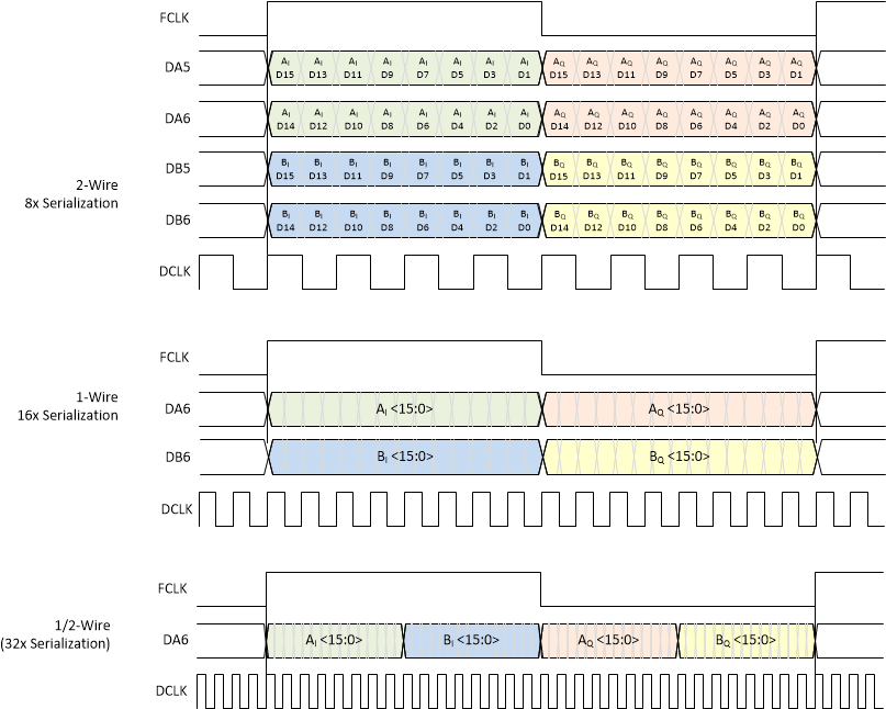
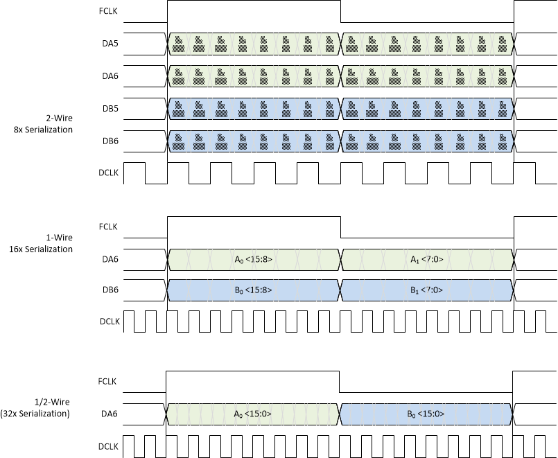
When using decimation, the output data is formatted as shown in Figure 8-34 (complex decimation) and Figure 8-35 (real decimation). The interface data rates for 2-, 1- and 1/2-wire for complex output for different decimation settings are shown in Table 8-4.
 Figure 8-34 Output Data Format in Complex Decimation
Table 8-4 illustrates the output interface data rate along with the corresponding DCLK/DCLKIN and FCLK frequencies based on output resolution (R), number of SCMOS lanes (L) and complex decimation setting (N).
Furthermore the table shows an actual lane rate example for the 2-, 1- and 1/2-wire interface, 16-bit output resolution and complex decimation by 16.
| DECIMATION SETTING | ADC SAMPLING RATE | OUTPUT RESOLUTION | # of WIRES | FCLK | DCLKIN, DCLK | DA/B5,6 |
|---|---|---|---|---|---|---|
| N | FS | R | L | FS / N | [DA/B5,6] / 2 | FS x 2 x R / L / N |
| 16 | 65 MSPS | 16 | 2 | 4..0625 MHz | 32.5 MHz | 65 MHz |
| 1 | 65 MHz | 130 MHz | ||||
| 62.5 MSPS | 1/2 | 3.90625 MHz | 125 MHz | 250 MHz |
 Figure 8-35 Output Data Format in Real Decimation
Table 8-5 illustrates the output interface data rate along with the corresponding DCLK/DCLKIN and FCLK frequencies based on output resolution (R), number of SCMOS lanes (L) and real decimation setting (M).
Furthermore the table shows an actual lane rate example for the 2-, 1- and 1/2-wire interface, 16-bit output resolution and real decimation by 16.
| DECIMATION SETTING | ADC SAMPLING RATE | OUTPUT RESOLUTION | # of WIRES | FCLK | DCLKIN, DCLK | DA/B5,6 |
|---|---|---|---|---|---|---|
| M | FS | R | L | FS / M / 2 (L = 2) FS / M (L = 1, 1/2) | [DA/B5,6] / 2 | FS x R / L / M |
| 16 | 65 MSPS | 16 | 2 | 2.03125 MHz | 16.25 MHz | 32.5 MHz |
| 1 | 4.0625 MHz | 32.5 MHz | 65 MHz | |||
| 1/2 | 65 MHz | 130 MHz |