ZHCSJ60D November   2018  – December 2019 TPS1HA08-Q1

PRODUCTION DATA.  

  1. 特性
  2. 应用
  3. 说明
    1.     简化原理图
  4. 修订历史记录
  5. Device Comparison Table
  6. Pin Configuration and Functions
    1.     Pin Functions
    2. 6.1 Recommended Connections for Unused Pins
  7. Specifications
    1. 7.1 Absolute Maximum Ratings
    2. 7.2 ESD Ratings
    3. 7.3 Recommended Operating Conditions
    4. 7.4 Thermal Information
    5. 7.5 Electrical Characteristics
    6. 7.6 Switching Characteristics
    7. 7.7 SNS Timing Characteristics
    8. 7.8 Typical Characteristics
  8. Parameter Measurement Information
  9. Detailed Description
    1. 9.1 Overview
      1. 9.1.1 Device Nomenclature
    2. 9.2 Functional Block Diagram
    3. 9.3 Feature Description
      1. 9.3.1 Protection Mechanisms
        1. 9.3.1.1 Thermal Shutdown
        2. 9.3.1.2 Current Limit
          1. 9.3.1.2.1 Current Limit Foldback
          2. 9.3.1.2.2 Selectable Current Limit Threshold
          3. 9.3.1.2.3 Undervoltage Lockout (UVLO)
          4. 9.3.1.2.4 VBB during Short-to-Ground
        3. 9.3.1.3 Energy Limit
        4. 9.3.1.4 Voltage Transients
          1. 9.3.1.4.1 Load Dump
          2. 9.3.1.4.2 Driving Inductive and Capacitive Loads
        5. 9.3.1.5 Reverse Battery
        6. 9.3.1.6 Fault Event – Timing Diagrams
      2. 9.3.2 Diagnostic Mechanisms
        1. 9.3.2.1 VOUT Short-to-Battery and Open-Load
          1. 9.3.2.1.1 Detection With Switch Enabled
          2. 9.3.2.1.2 Detection With Switch Disabled
        2. 9.3.2.2 SNS Output
          1. 9.3.2.2.1 RSNS Value
            1. 9.3.2.2.1.1 High Accuracy Load Current Sense
            2. 9.3.2.2.1.2 SNS Output Filter
        3. 9.3.2.3 ST Pin
        4. 9.3.2.4 Fault Indication and SNS Mux
        5. 9.3.2.5 Resistor Sharing
        6. 9.3.2.6 High-Frequency, Low Duty-Cycle Current Sensing
      3. 9.3.3 Enable Watchdog
    4. 9.4 Device Functional Modes
      1. 9.4.1 Off
      2. 9.4.2 Standby
      3. 9.4.3 Diagnostic
      4. 9.4.4 Standby Delay
      5. 9.4.5 Active
      6. 9.4.6 Fault
  10. 10Application and Implementation
    1. 10.1 Application Information
      1. 10.1.1 Ground Protection Network
      2. 10.1.2 Interface With Microcontroller
      3. 10.1.3 I/O Protection
      4. 10.1.4 Inverse Current
      5. 10.1.5 Loss of GND
      6. 10.1.6 Automotive Standards
        1. 10.1.6.1 ISO7637-2
        2. 10.1.6.2 AEC – Q100-012 Short Circuit Reliability
      7. 10.1.7 Thermal Information
    2. 10.2 Typical Application
      1. 10.2.1 Design Requirements
      2. 10.2.2 Detailed Design Procedure
        1. 10.2.2.1 Thermal Considerations
        2. 10.2.2.2 Diagnostics
          1. 10.2.2.2.1 Selecting the RISNS Value
      3. 10.2.3 Application Curves
  11. 11Power Supply Recommendations
  12. 12Layout
    1. 12.1 Layout Guidelines
    2. 12.2 Layout Example
  13. 13器件和文档支持
    1. 13.1 器件支持
      1. 13.1.1 相关文档
    2. 13.2 商标
    3. 13.3 静电放电警告
    4. 13.4 Glossary
  14. 14机械、封装和可订购信息

Typical Characteristics

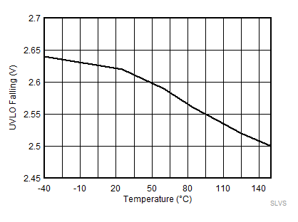
TPS1HA08-Q1 SLVSDF0_DG1.gif
VBB = 13.5 V to 0 V ROUT = 1 kΩ VDIAG__EN = 0 V
VEN = 5 V
Figure 3. Falling Undervoltage Lockout (VUVLOF) vs Temperature
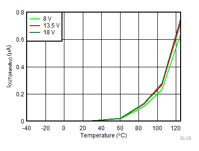
TPS1HA08-Q1 SLVSDF0_DG3.gif
VOUT = 0 V VEN = 0 V VDIAG_EN = 0 V
Figure 5. Output Leakage Current (IOUT(standby)) vs Temperature
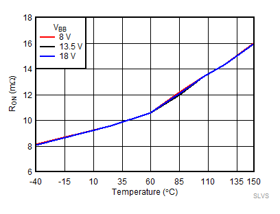
TPS1HA08-Q1 SLVSDF0_DG5.gif
IOUT = 200 mA VEN = 5 V VDIAG_EN = 0 V
RSNS = 1 kΩ
Figure 7. On Resistance (RON) vs Temperature
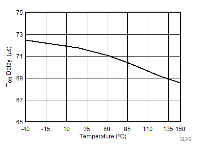
TPS1HA08-Q1 SLVSDF0_DG8.gif
ROUT = 2.6 Ω VEN = 0 V to 5 V VDIAG_EN = 0 V
RSNS = 1 kΩ VBB = 13.5 V
Figure 9. Turn-on Delay Time (tDR) vs Temperature
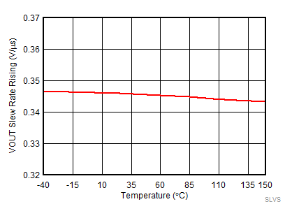
TPS1HA08-Q1 SLVSDF0_DG10.gif
ROUT = 2.6 Ω VEN = 0 V to 5 V VDIAG_EN = 0 V
RSNS = 1 kΩ VBB = 13.5 V
Figure 11. VOUT Slew Rate Rising (SRR) vs Temperature
TPS1HA08-Q1 SLVSDF0_DG12.gif
ROUT = 2.6 Ω VEN = 0 V to 5 V VDIAG_EN = 0 V
RSNS = 1 kΩ VBB = 13.5 V
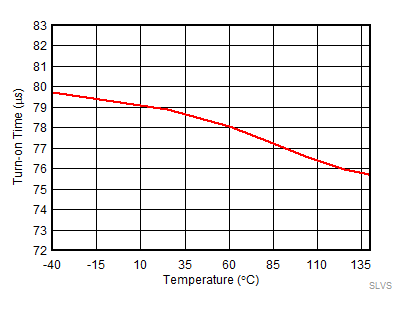
Figure 13. Turn-on Time (tON) vs Temperature
TPS1HA08-Q1 SLVSDF0_DG14.gif
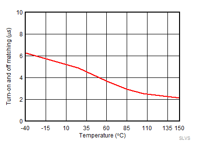
ROUT = 2.6 Ω VEN = 0 V to 5 V and 5 V to 0 V VDIAG_EN = 0 V
RSNS = 1 kΩ VBB = 13.5 V
Figure 15. Turn-on and Turn-off Matching (tON - tOFF) vs Temperature
TPS1HA08-Q1 SLVSDF0_DG16.gif
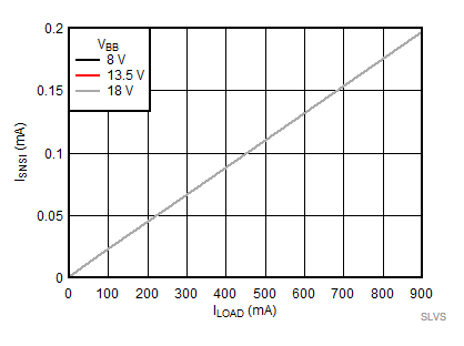
VSEL1 = VSEL2 = 0 V VEN = 5 V VDIAG_EN = 5 V
RSNS = 1 kΩ TA = 25°C
Figure 17. Current Sense Output Current (ISNSI) vs Load Current (IOUT) across VBB
TPS1HA08-Q1 SLVSDF0_DG18.gif
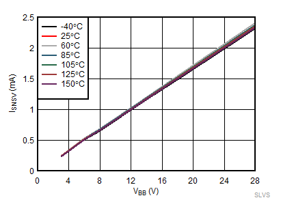
VSEL1 = VSEL2 = 5 V VEN = 0 V VDIAG_EN = 5 V
RSNS = 1 kΩ IOUT = 0 A
Figure 19. Voltage Sense Output Current (ISNSV) vs VBB
TPS1HA08-Q1 SLVSDF0_DG20.gif
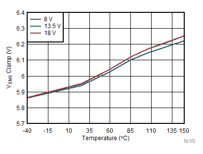
VSEL1 = VSEL2 = 0 V VEN = 5 V VDIAG_EN = 5 V
RSNS = 10 kΩ IOUT = 4 A
Figure 21. Sense Pin Clamp Voltage (VSNSCLAMP) vs Temperature
TPS1HA08-Q1 SLVSDF0_DG22.gif
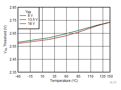
VEN = 0 V VOUT = 0 V to 5 V IOUT = 0 A
VDIAG_EN= 5 V VSEL1 = VSEL2 = 0 V
Figure 23. Open Load Detection Voltage (VOL) vs Temperature
TPS1HA08-Q1 SLVSDF0_DG24.gif
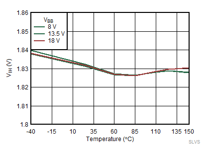
VEN = 0 V to 3.3 V VOUT = 0 V VDIAG_EN = 0 V
ROUT = 1 kΩ
Figure 25. VIH vs Temperature
TPS1HA08-Q1 SLVSDF0_DG26.gif
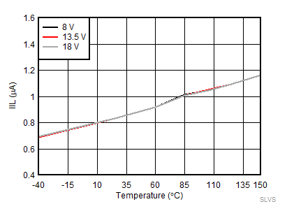
VEN = 0.8 V VOUT = 0 V VDIAG_EN = 0 V
ROUT = 1 kΩ
Figure 27. IIL vs Temperature
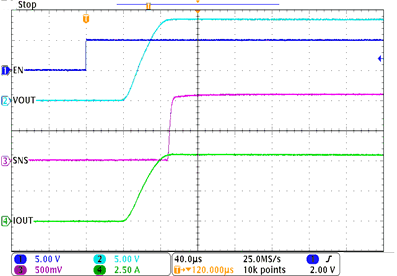
TPS1HA08-Q1 SS1_TEK00289_SLVSD84.gif
ROUT = 2.6 Ω RSNS = 1 kΩ VDIA_EN = 5 V
VSEL1 = VSEL2 = 0 V
Figure 29. Turn-on Time (tON)
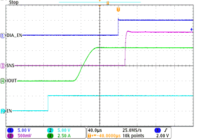
TPS1HA08-Q1 SS3_TEK00290_SLVSD84.gif
ROUT = 2.6 Ω RSNS = 1 kΩ VDIA_EN= 0 V to 5 V
VSEL1 = VSEL2 = 0 V
Figure 31. ISNS Settling Time (tSNSION1) on DIA_EN Transition
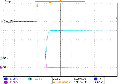
TPS1HA08-Q1 SS6_TEK00294_SLVSD84.gif
VOUT = VBB RSNS = 1 kΩ VSEL1 = VSEL2 = 0 V
VEN = 0 V VDIAG_EN = 5 V
Figure 33. Open Load Detection Time (tOL2) on Rising DIAG_EN
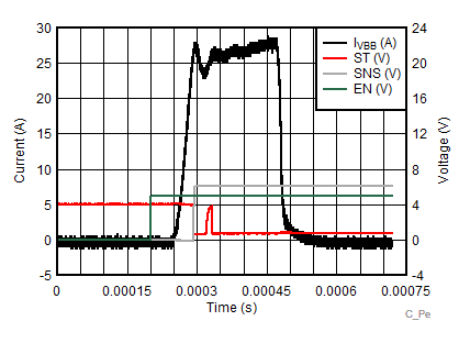
TPS1HA08-Q1 C_PermShort.gif
VBB = 13.5 V C Device Version VOUT = 0 V
VEN = 0 V to 5 V TA = 25°C
Figure 35. Short Circuit Behavior with C Device Version
TPS1HA08-Q1 SLVSDF0_DG2.gif
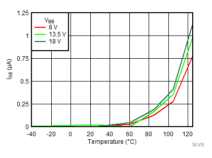
VOUT = 0 V VEN = 0 V VDIAG_EN = 0 V
Figure 4. Standby Current (ISB) vs Temperature
TPS1HA08-Q1 SLVSDF0_DG4.gif
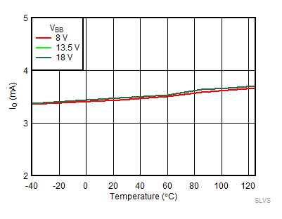
IOUT = 0 A VEN = 5 V VDIAG_EN = 5 V
RSNS = 1 kΩ VSEL1 = VSEL2 = 0 V
Figure 6. Quiescent Current (IQ) vs Temperature
TPS1HA08-Q1 SLVSDF0_DG6.gif
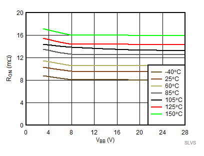
IOUT = 200 mA VEN = 5 V VDIAG_EN = 0 V
RSNS = 1 kΩ VBB = 13.5 V
Figure 8. On Resistance (RON) vs VBB
TPS1HA08-Q1 SLVSDF0_DG9.gif
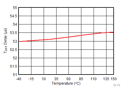
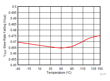
ROUT = 2.6 Ω VEN = 5 V to 0 V VDIAG_EN = 0 V
RSNS = 1 kΩ VBB = 13.5 V
Figure 10. Turn-off Delay Time (tDF) vs Temperature
TPS1HA08-Q1 SLVSDF0_DG11.gif
ROUT = 2.6 Ω VEN = 5 V to 0 V VDIAG_EN = 0 V
RSNS = 1 kΩ VBB = 13.5 V
Figure 12. VOUT Slew Rate Falling (SRF) vs Temperature
TPS1HA08-Q1 SLVSDF0_DG13.gif
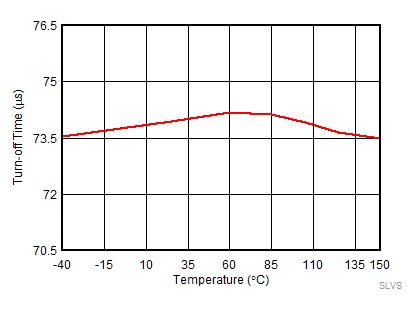
ROUT = 2.6 Ω VEN = 5 V to 0 V VDIAG_EN = 0 V
RSNS = 1 kΩ VBB = 13.5 V
Figure 14. Turn-off Time (tOFF) vs Temperature
TPS1HA08-Q1 SLVSDF0_DG15.gif
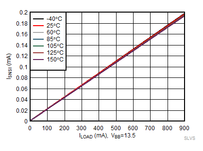
VSEL1 = VSEL2 = 0 V VEN = 5 V VDIAG_EN = 5 V
RSNS = 1 kΩ VBB = 13.5 V
Figure 16. Current Sense Output Current (ISNSI ) vs Load Current (IOUT) across Temperature
TPS1HA08-Q1 SLVSDF0_DG17.gif
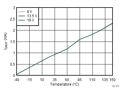
VSEL1 = 5 V VSEL2 = 0 V VDIAG_EN = 5 V
RSNS = 1 kΩ VEN = 0 V
Figure 18. Temperature Sense Output Current (ISNST) vs Temperature
TPS1HA08-Q1 SLVSDF0_DG19.gif
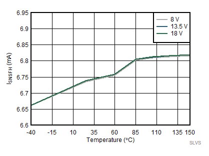
VSEL1 = VSEL2 = 0 V VEN = 0 V VDIAG_EN = 5 V
RSNS = 500 Ω VOUT Floating
Figure 20. Fault High Output Current (ISNSFH) vs Temperature
TPS1HA08-Q1 SLVSDF0_DG21.gif
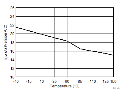
VBB = 13.5 V VOUT = 0 V VDIAG_EN = 0 V
Device Version C VEN = 5 V VLATCH = 5 V
Figure 22. Current Limit (ICL) vs Temperature
TPS1HA08-Q1 SLVSDF0_DG23.gif
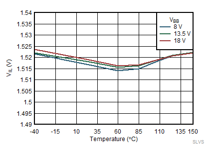
VEN = 3.3 V to 0 V VOUT = 0 V VDIAG_EN = 0 V
ROUT = 1 kΩ
Figure 24. VIL vs Temperature
TPS1HA08-Q1 SLVSDF0_DG25.gif
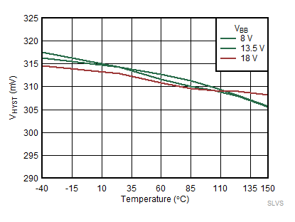
VEN = 0 V to 3.3 V and 3.3 V to 0 V VOUT = 0 V VDIAG_EN = 0 V
ROUT = 1 kΩ
Figure 26. VIHYS vs Temperature
TPS1HA08-Q1 SLVSDF0_DG27.gif
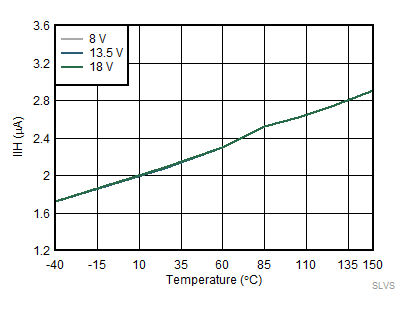
VEN = 2 V VOUT = 0 V VDIAG_EN = 0 V
ROUT = 1 kΩ
Figure 28. IIH vs Temperature
TPS1HA08-Q1 SS2_TEK00288_SLVSD84.gif
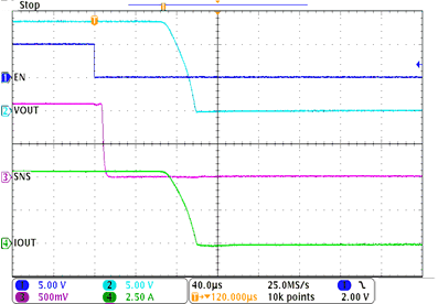
ROUT = 2.6 Ω RSNS = 1 kΩ VDIA_EN = 5 V
VSEL1 = VSEL2 = 0 V
Figure 30. Turn-off Time (tOFF) and Sense Settle Time (tSNSION2)
TPS1HA08-Q1 SS4_TEK00291_SLVSD84.gif
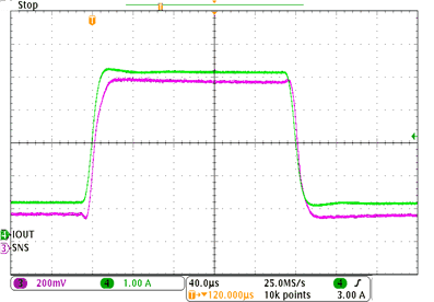
IOUT = 1 A to 5 A RSNS = 1 kΩ VDIA_EN = 5 V
VSEL1 = VSEL2 = 0 V
Figure 32. ISNS Settling Time (tSETTLEH) on Rising Load Step
TPS1HA08-Q1 BPermShort.gif
VBB = 13.5 V B Device Version VOUT = 0 V
VEN = 0 V to 5 V TA = 25°C
Figure 34. Short Circuit Behavior with B Device Version
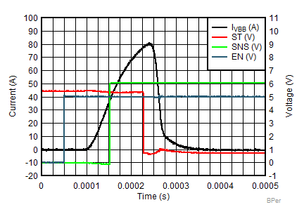
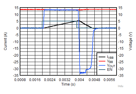
TPS1HA08-Q1 Inductive Repetitive.gif
VBB = 13.5 V TA = 125°C LOUT = 5 mH
VEN = 0 V to 5 V, 5 V to 0 V
Figure 36. Inductive Load Demagnetization