ZHCSHZ8B april 2018 – february 2023 TPS62147 , TPS62148
PRODUCTION DATA
- 1 特性
- 2 应用
- 3 说明
- 4 Revision History
- 5 Device Comparison Table
- 6 Pin Configuration and Functions
- 7 Specifications
- 8 Parameter Measurement Information
-
9 Detailed Description
- 9.1 Overview
- 9.2 Functional Block Diagram
- 9.3 Feature Description
- 9.4
Device Functional Modes
- 9.4.1 Pulse Width Modulation (PWM) Operation
- 9.4.2 Power Save Mode Operation (PWM/PFM)
- 9.4.3 100% Duty-Cycle Operation
- 9.4.4 Current Limit And Short Circuit Protection (for TPS62148)
- 9.4.5 HICCUP Current Limit And Short Circuit Protection (for TPS62147)
- 9.4.6 Soft Start / Tracking (SS/TR)
- 9.4.7 Output Discharge Function (TPS62148 only)
- 9.4.8 Starting into a Pre-Biased Load
- 10Application and Implementation
- 11Device and Documentation Support
- 12Mechanical, Packaging, and Orderable Information
10.3.1 LED Power Supply
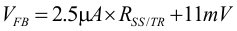
The TPS62147, TPS62148 can be used as a power supply for power LEDs. The FB pin can be easily set down to lower values than nominal by using the SS/TR pin. With that, the voltage drop on the sense resistor is low to avoid excessive power loss. Because this pin provides 2.5 µA, the feedback pin voltage can be adjusted by an external resistor per Equation 20. This drop, proportional to the LED current, is used to regulate the output voltage (anode voltage) to a proper level to drive the LED. Both analog and PWM dimming are supported with the TPS62147, TPS62148.
Figure 10-80 shows an application circuit, tested with analog dimming:
 Figure 10-80 Single Power LED Supply
The resistor at SS/TR defines the FB voltage. It is set to 350 mV by R5 = 140 kΩ using Equation 20. This cuts the losses on R4 to half from the nominal 0.7 V of feedback voltage while it still provides good accuracy.
The device supplies a constant current set by resistor R4 from FB to GND. The minimum input voltage has to be rated according the forward voltage needed by the LED used. More information is available in the Application Note SLVA451.