ZHCSH62B December 2017 – October 2019 LM76002-Q1 , LM76003-Q1
PRODUCTION DATA.
- 1 特性
- 2 应用
- 3 说明
- 4 修订历史记录
- 5 Pin Configuration and Functions
- 6 Specifications
-
7 Detailed Description
- 7.1 Overview
- 7.2 Functional Block Diagram
- 7.3
Feature Description
- 7.3.1 Fixed-Frequency, Peak-Current-Mode Control
- 7.3.2 Light Load Operation Modes — PFM and FPWM
- 7.3.3 Adjustable Output Voltage
- 7.3.4 Enable (EN Pin) and UVLO
- 7.3.5 Internal LDO, VCC UVLO, and Bias Input
- 7.3.6 Soft Start and Voltage Tracking (SS/TRK)
- 7.3.7 Adjustable Switching Frequency (RT) and Frequency Synchronization
- 7.3.8 Minimum On-Time, Minimum Off-Time, and Frequency Foldback at Dropout Conditions
- 7.3.9 Internal Compensation and CFF
- 7.3.10 Bootstrap Voltage and VBOOT UVLO (BOOT Pin)
- 7.3.11 Power Good and Overvoltage Protection (PGOOD)
- 7.3.12 Overcurrent and Short-Circuit Protection
- 7.3.13 Thermal Shutdown
- 7.4 Device Functional Modes
-
8 Application and Implementation
- 8.1 Application Information
- 8.2
Typical Applications
- 8.2.1 Design Requirements
- 8.2.2
Detailed Design Procedure
- 8.2.2.1 Custom Design With WEBENCH® Tools
- 8.2.2.2 Output Voltage Setpoint
- 8.2.2.3 Switching Frequency
- 8.2.2.4 Input Capacitors
- 8.2.2.5 Inductor Selection
- 8.2.2.6 Output Capacitor Selection
- 8.2.2.7 Feed-Forward Capacitor
- 8.2.2.8 Bootstrap Capacitors
- 8.2.2.9 VCC Capacitors
- 8.2.2.10 BIAS Capacitors
- 8.2.2.11 Soft-Start Capacitors
- 8.2.2.12 Undervoltage Lockout Setpoint
- 8.2.2.13 PGOOD
- 8.2.2.14 Synchronization
- 8.2.3 Application Curves
- 9 Power Supply Recommendations
- 10Layout
- 11器件和文档支持
- 12机械、封装和可订购信息
7.3.1 Fixed-Frequency, Peak-Current-Mode Control
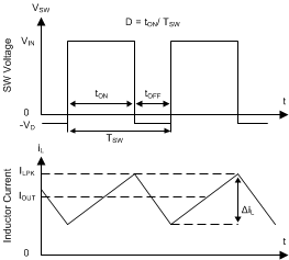
The following operation description of the LM76002-Q1/LM76003-Q1 refers to the Functional Block Diagram and to the waveforms in Figure 10. The LM76002-Q1/LM76003-Q1 supplies a regulated output voltage by turning on the internal high side (HS) and low side (LS) NMOS switches with varying duty cycle (D). During high-side switch on-time tON, the SW pin voltage VSW swings up to approximately VIN, and the inductor current iL increase with linear slope. The HS switch is off by the control logic. During the HS switch off-time, tOFF, the LS switch is turned on. Inductor current discharges through the LS switch, which forces the VSW to swing below ground by the voltage drop across the LS switch. The regulator loop adjusts the duty cycle to maintain a constant output voltage. The control parameter of buck converter is defined as duty cycle D = tON / tSW. In an ideal buck converter, where losses are ignored, D is proportional to the output voltage and inversely proportional to the input voltage: D = VOUT / VIN.
 Figure 10. SW Node and Inductor Current Waveforms in
Continuous Conduction Mode
The LM76002-Q1/LM76003-Q1 synchronous buck converter employs peak current-mode control topology. A voltage-feedback loop is used to get accurate DC-voltage regulation by adjusting the peak current command based on voltage offset. The peak inductor current is sensed from the HS switch and compared to the peak current to control the on-time of the HS switch. The voltage feedback loop is internally compensated, which allows command for fewer external components, makes it easy to design, and provides stable operation with almost any combination of output capacitors. The regulator operates with fixed switching frequency in continuous conduction mode (CCM) and discontinuous conduction mode (DCM). At very light load, the LM76002-Q1/LM76003-Q1 operates in PFM to maintain high efficiency, and the switching frequency decreases with reduced load current.