ZHCSFP8C December 2015 – September 2016 LP5912-Q1
PRODUCTION DATA.
- 1 特性
- 2 应用
- 3 说明
- 4 修订历史记录
- 5 Voltage Options
- 6 Pin Configuration and Functions
- 7 Specifications
- 8 Detailed Description
- 9 Applications and Implementation
- 10Power Supply Recommendations
- 11Layout
- 12器件和文档支持
- 13机械、封装和可订购信息
7 Specifications
7.1 Absolute Maximum Ratings
over operating free-air temperature range (unless otherwise noted)(1)(2)| MIN | MAX | UNIT | ||
|---|---|---|---|---|
| VIN | Input voltage | –0.3 | 7 | V |
| VOUT | Output voltage | –0.3 | 7 | V |
| VEN | Enable input voltage | –0.3 | 7 | V |
| VPG | Power Good (PG) pin OFF voltage | –0.3 | 7 | V |
| TJ | Junction temperature | 150 | °C | |
| PD | Continuous power dissipation(3) | Internally Limited | W | |
| Tstg | Storage temperature | –65 | 150 | °C |
(1) Stresses beyond those listed under Absolute Maximum Ratings may cause permanent damage to the device. These are stress ratings only, which do not imply functional operation of the device at these or any other conditions beyond those indicated under Recommended Operating Conditions. Exposure to absolute-maximum-rated conditions for extended periods may affect device reliability.
(2) All voltages are with respect to the GND pin.
(3) Internal thermal shutdown circuitry protects the device from permanent damage.
7.2 ESD Ratings
| VALUE | UNIT | |||
|---|---|---|---|---|
| V(ESD) | Electrostatic discharge | Human-body model (HBM), per AEC Q100-002(1) | ±2000 | V |
| Charged-device model (CDM), per AEC Q100-011 | ±1000 | |||
(1) AEC Q100-002 indicates that HBM stressing shall be in accordance with the ANSI/ESDA/JEDEC JS-001 specification.
7.3 Recommended Operating Conditions
over operating free-air temperature range (unless otherwise noted)(1)| MIN | MAX | UNIT | ||
|---|---|---|---|---|
| VIN | Input supply voltage | 1.6 | 6.5 | V |
| VOUT | Output voltage | 0.8 | 5.5 | V |
| VEN | Enable input voltage | 0 | VIN | V |
| VPG | PG pin OFF voltage | 0 | 6.5 | V |
| IOUT | Output current | 0 | 500 | mA |
| TJ-MAX-OP | Operating junction temperature(2) | –40 | 125 | °C |
(1) All voltages are with respect to the GND pin.
(2) TJ-MAX-OP = (TA(MAX) + (PD(MAX) × RθJA )).
7.4 Thermal Information
| THERMAL METRIC(1) | LP5912-Q1 | UNIT | |
|---|---|---|---|
| DRV (WSON) | |||
| 6 PINS | |||
| RθJA | Junction-to-ambient thermal resistance, High-K(2) | 71.2(3) | °C/W |
| RθJC(top) | Junction-to-case (top) thermal resistance | 93.7 | °C/W |
| RθJB | Junction-to-board thermal resistance | 40.7 | °C/W |
| ψJT | Junction-to-top characterization parameter | 2.5 | °C/W |
| ψJB | Junction-to-board characterization parameter | 41.1 | °C/W |
| ψJC(bot) | Junction-to-case (bottom) thermal resistance | 11.2 | °C/W |
(1) For more information about traditional and new thermal metrics, see the Semiconductor and IC Package Thermal Metrics application report, SPRA953.
(2) Thermal resistance value RθJA is based on the EIA/JEDEC High-K printed circuit board defined by: JESD51-7 - High Effective Thermal Conductivity Test Board for Leaded Surface Mount Packages.
(3) The PCB for the WSON (DRV) package RθJA includes two (2) thermal vias under the exposed thermal pad per EIA/JEDEC JESD51-5.
7.5 Electrical Characteristics
VIN = VOUT(NOM) + 0.5 V or 1.6 V, whichever is greater; VEN = 1.3 V, CIN = 1 µF, COUT = 1 µF, IOUT = 1 mA (unless otherwise stated).(1)(2)(3)| PARAMETER | TEST CONDITIONS | MIN | TYP | MAX | UNIT | |
|---|---|---|---|---|---|---|
| OUTPUT VOLTAGE | ||||||
| ΔVOUT | Output voltage tolerance | For VOUT(NOM) ≥ 3.3 V: VOUT(NOM) + 0.5 V ≤ VIN ≤ 6.5 V, IOUT = 1 mA to 500 mA |
–2% | 2% | ||
| For 1.1 V ≤ VOUT(NOM) < 3.3 V: VOUT(NOM) + 0.5 V ≤ VIN ≤ 6.5 V, IOUT = 1 mA to 500 mA |
–3% | 3% | ||||
| For VOUT(NOM) < 1.1 V: 1.6 V ≤ VIN ≤ 6.5 V, IOUT = 1 mA to 500 mA |
||||||
| Line regulation | For VOUT(NOM) ≥ 1.1 V: VOUT(NOM) + 0.5 V ≤ VIN ≤ 6.5 V |
0.8 | %/V | |||
| For VOUT(NOM) < 1.1 V: 1.6 V ≤ VIN ≤ 6.5 V |
||||||
| Load regulation | IOUT = 1 mA to 500 mA | 0.0022 | %/mA | |||
| CURRENT LEVELS | ||||||
| ISC | Short-circuit current limit | TJ = 25°C, see(4) | 700 | 900 | 1100 | mA |
| IRO | Reverse leakage current(5) | VIN < VOUT | 10 | 150 | µA | |
| IQ | Quiescent current(6) | VEN = 1.3 V, IOUT = 0 mA | 30 | 55 | µA | |
| VEN = 1.3 V, IOUT = 500 mA | 400 | 600 | ||||
| IQ(SD) | Quiescent current, shutdown mode(6) | VEN = 0 V –40°C ≤ TJ ≤ 85°C |
0.2 | 1.5 | µA | |
| VEN = 0 V | 0.2 | 5 | ||||
| IG | Ground current(7) | VEN = 1.3 V, IOUT = 0 mA | 35 | µA | ||
| VDO DROPOUT VOLTAGE | ||||||
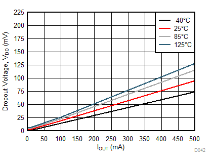
| VDO | Dropout voltage(8) | IOUT = 500 mA, 1.6 V ≤ VOUT(NOM) < 3.3 V | 170 | 250 | mV | |
| IOUT = 500 mA, 3.3 V ≤ VOUT(NOM) ≤ 5.5 V | 95 | 180 | mV | |||
| VIN to VOUT RIPPLE REJECTION | ||||||
| PSRR | Power Supply Rejection Ratio(10) | ƒ = 100 Hz, VOUT ≥ 1.1 V, IOUT = 20 mA | 80 | dB | ||
| ƒ = 1 kHz, VOUT ≥ 1.1 V, IOUT = 20 mA | 75 | |||||
| ƒ = 10 kHz, VOUT ≥ 1.1 V, IOUT = 20 mA | 65 | |||||
| ƒ = 100 kHz, VOUT ≥ 1.1 V, IOUT = 20 mA | 40 | |||||
| ƒ = 100 Hz, 0.8 V < VOUT < 1.1 V, IOUT = 20 mA | 65 | |||||
| ƒ = 1 kHz, 0.8 V < VOUT < 1.1 V, IOUT = 20 mA | 65 | |||||
| ƒ = 10 kHz, 0.8 V < VOUT < 1.1 V, IOUT = 20 mA | 65 | |||||
| ƒ = 100 kHz, 0.8 V < VOUT < 1.1 V, IOUT = 20 mA | 40 | |||||
| OUTPUT NOISE VOLTAGE | ||||||
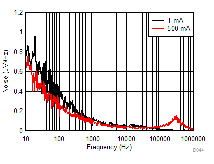
| eN | Noise voltage | IOUT = 1 mA, BW = 10 Hz to 100 kHz | 12 | µVRMS | ||
| IOUT = 500 mA, BW = 10 Hz to 100 kHz | 12 | |||||
| THERMAL SHUTDOWN | ||||||
| TSD | Thermal shutdown temperature | 160 | °C | |||
| THYS | Thermal shutdown hysteresis | 15 | °C | |||
| LOGIC INPUT THRESHOLDS | ||||||
| VEN(OFF) | OFF threshold | VIN = 1.6 V to 6.5 V VEN falling until device is disabled |
0.3 | V | ||
| VEN(ON) | ON threshold | 1.6 V ≤ VIN ≤ 6.5 V VEN rising until device is enabled |
1.3 | |||
| IEN | Input current at EN pin(9) | VEN = 6.5 V, VIN = 6.5 V | 2.5 | µA | ||
| VEN = 0 V, VIN = 3.3 V | 0.001 | |||||
| PGHTH | PG high threshold (% of nominal VOUT) | 94% | ||||
| PGLTH | PG low threshold (% of nominal VOUT) | 90% | ||||
| VOL(PG) | PG pin low-level output voltage | VOUT < PGLTH, sink current = 1 mA | 100 | mV | ||
| IlKG(PG) | PG pin leakage current | VOUT < PGHTH, VPG = 6.5 V | 1 | µA | ||
| tPGD | PG delay time | Time from VOUT > PG threshold to PG toggling | 140 | µs | ||
| TRANSITION CHARACTERISTICS | ||||||
| ΔVOUT | Line transients(10) | For VIN ↑ and VOUT(NOM) ≥ 1.1 V: VIN = (VOUT(NOM) + 0.5 V) to (VOUT(NOM) + 1.1 V), VIN trise = 30 µs |
1 | mV | ||
| For VIN ↑ and VOUT(NOM) < 1.1 V: VIN = 1.6 V to 2.2 V, VIN trise = 30 µs |
||||||
| For VIN ↓ and VOUT(NOM) ≥ 1.1 V: VIN = (VOUT(NOM) + 1.1 V) to (VOUT(NOM) + 0.5 V) VIN tfall = 30 µs |
–1 | |||||
| For VIN ↓ and VOUT(NOM) < 1.1 V: VIN = 2.2 V to 1.6 V VIN tfall = 30 µs |
||||||
| Load transients(10) | IOUT = 5 mA to 500 mA IOUT trise = 10 µs |
–45 | mV | |||
| IOUT = 500 mA to 5 mA IOUT tfall = 10 µs |
45 | |||||
| Overshoot on start-up(10) | Stated as a percentage of VOUT(NOM) | 5% | ||||
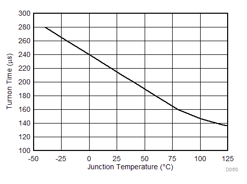
| tON | Turnon time | From VEN > VEN(ON) to VOUT = 95% of VOUT(NOM) | 200 | µs | ||
| OUTPUT AUTO DISCHARGE RATE | ||||||
| RAD | Output discharge pulldown resistance | VEN = 0 V, VIN = 3.6 V | 100 | Ω | ||
(1) All voltages are with respect to the device GND pin, unless otherwise stated.
(2) Minimum and maximum limits are ensured through test, design, or statistical correlation over the junction temperature (TJ) range of –40°C to +125°C, unless otherwise stated. Typical values represent the most likely parametric norm at TA = 25°C, and are provided for reference purposes only.
(3) In applications where high power dissipation and/or poor package thermal resistance is present, the maximum ambient temperature may have to be derated. Maximum ambient temperature (TA-MAX) is dependent on the maximum operating junction temperature (TJ-MAX-OP = 125°C), the maximum power dissipation of the device in the application (PD-MAX), and the junction-to-ambient thermal resistance of the part/package in the application (RθJA), as given by the following equation: TA-MAX = TJ-MAX-OP – (RθJA × PD-MAX).
(4) Short-circuit current (ISC) is equivalent to current limit. To minimize thermal effects during testing, ISC is measured with VOUT pulled to 100 mV below its nominal voltage.
(5) Reverse current (IRO) is measured at the IN pin.
(6) Quiescent current is defined here as the difference in current between the input voltage source and the load at VOUT.
(7) Ground current is defined here as the total current flowing to ground as a result of all input voltages applied to the device (IQ + IEN).
(8) Dropout voltage (VDO) is the voltage difference between the input and the output at which the output voltage drops to 150 mV below its nominal value when VIN = VOUT + 0.5 V. Dropout voltage is not a valid condition for output voltages less than 1.6 V as compliance with the minimum operating voltage requirement cannot be assured.
(9) There is a 3-MΩ pulldown resistor between the EN pin and GND pin on the device.
(10) This specification is ensured by design.
7.6 Output and Input Capacitors
over operating free-air temperature range (unless otherwise noted)| PARAMETER | TEST CONDITIONS | MIN(1) | TYP | MAX | UNIT | |
|---|---|---|---|---|---|---|
| CIN | Input capacitance(2) | Capacitance for stability | 0.7 | 1 | µF | |
| COUT | Output capacitance(2) | 0.7 | 1 | 10 | µF | |
| ESR | Output voltage(2) | 5 | 500 | mΩ | ||
(1) The minimum capacitance must be greater than 0.5 μF over full range of operating conditions. The capacitor tolerance must be 30% or better over the full temperature range. The full range of operating conditions for the capacitor in the application must be considered during device selection to ensure this minimum capacitance specification is met. X7R capacitors are recommended however capacitor types X5R, Y5V, and Z5U may be used with consideration of the application conditions.
(2) This specification is verified by design.
7.7 Typical Characteristics
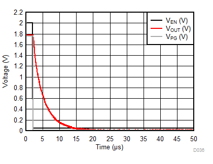
Unless otherwise stated: VIN = VOUT + 0.5 V, VEN = VIN, IOUT = 1 mA, CIN = 1 µF, COUT = 1 µF, TJ = 25°C, unless otherwise stated.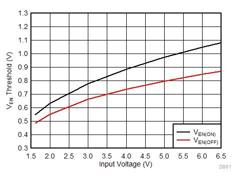
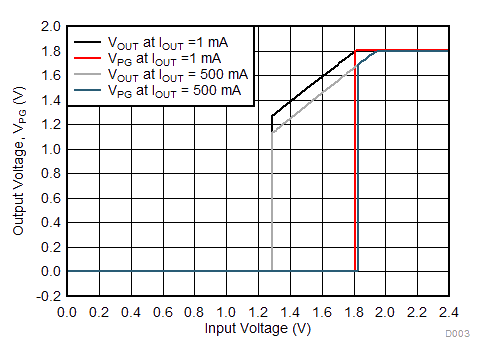
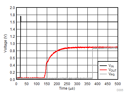
| VIN = 0 V to 1.6 V | IOUT = 1 mA | |

| VIN = 0 V to 2.3 V | IOUT = 1 mA | |
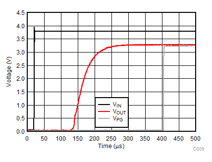
| VIN = 0 V to 3.8 V | IOUT = 1 mA | |
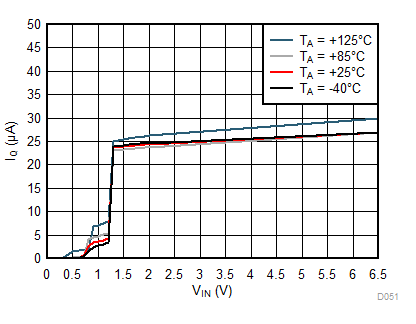
| IOUT = 0 mA |
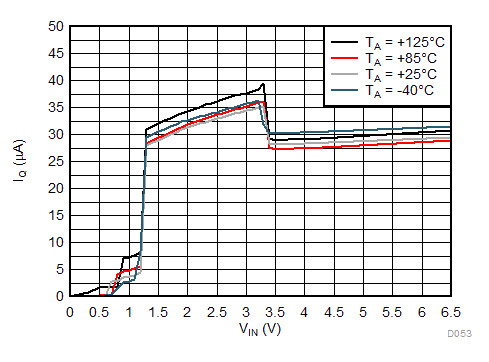
| IOUT = 0 mA | ||
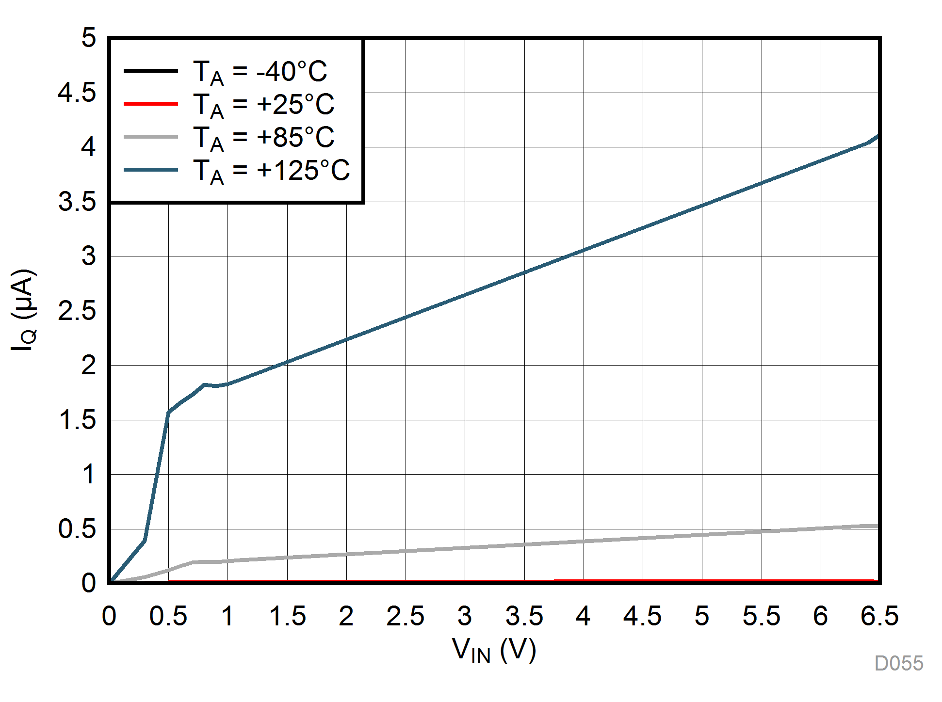
| VEN = 0 V |
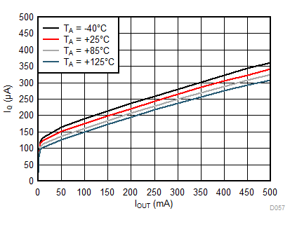
| VIN = 1.6 V |
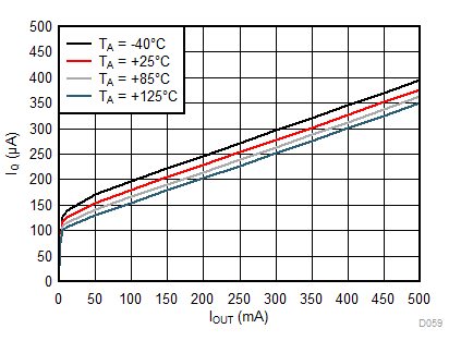
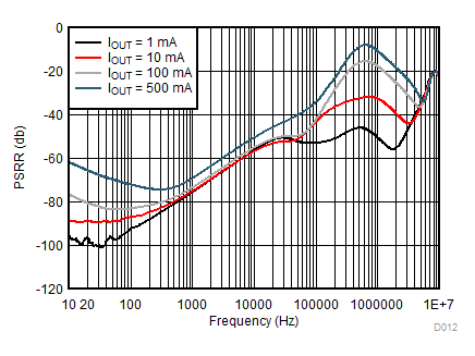
| VIN = 1.6 V | ||
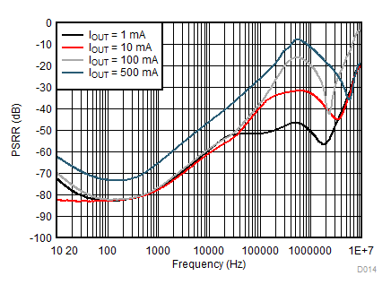
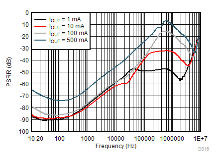
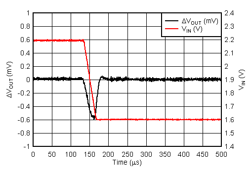
| VIN = 2.2 V to 1.6 V | tfall = 30 µs | |
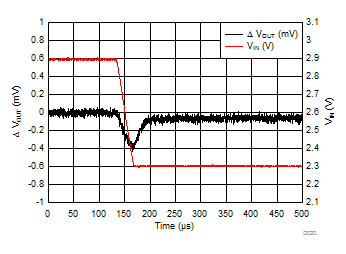
| VIN = 2.9 V to 2.3 V | tfall = 30 µs | |
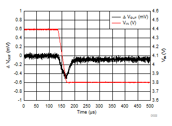
| VIN = 4.4 V to 3.8 V | tfall = 30 µs | |
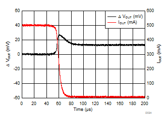
| VIN = 1.6 V | IOUT = 500 mA to 5 mA | tfall = 10 µs |
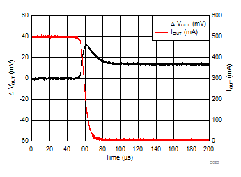
| IOUT = 500 mA to 5 mA | tfall = 10 µs | |
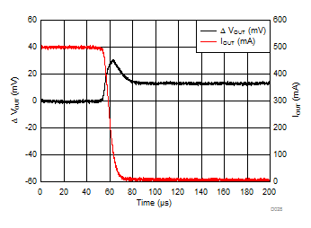
| IOUT = 500 mA to 5 mA | tfall = 10 µs | |
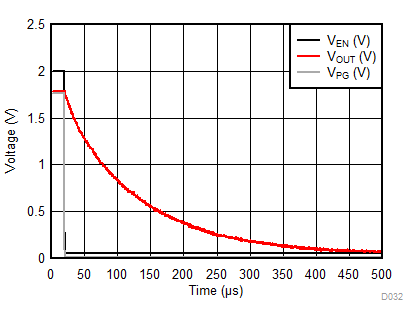
| IOUT = 0 mA | COUT = 1 µF |
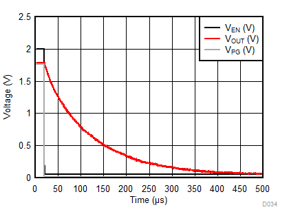
| IOUT = 1 mA | COUT = 1 µF |
| IOUT = 500 mA | COUT = 1 µF |
| IOUT = 0 mA (No Load) |
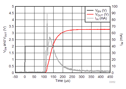
| CIN = Open | IOUT = 1 mA | COUT = 1 µF |
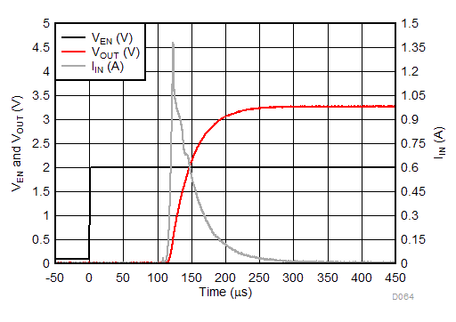
| CIN = Open | IOUT = 1 mA | COUT = 10 µF | ||
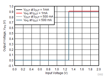
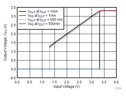
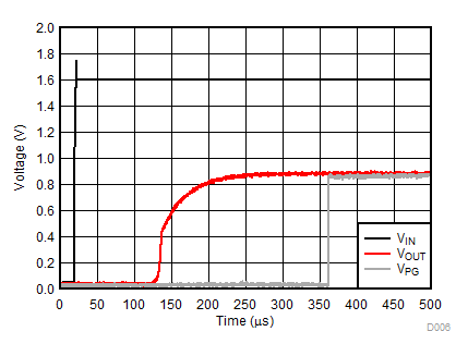
| VIN = 0 V to 1.6 V | IOUT = 500 mA | |
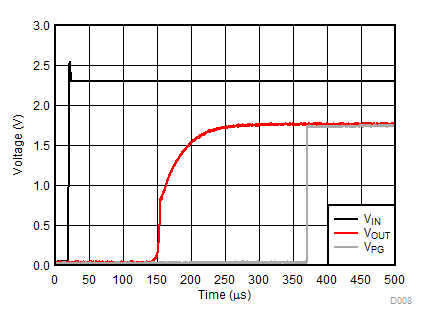
| VIN = 0 V to 2.3 V | IOUT = 500 mA | |
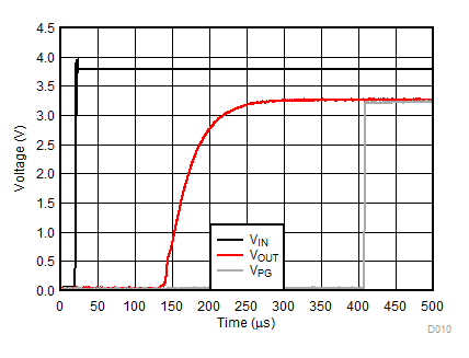
| VIN = 0 V to 3.8 V | IOUT = 500 mA | |
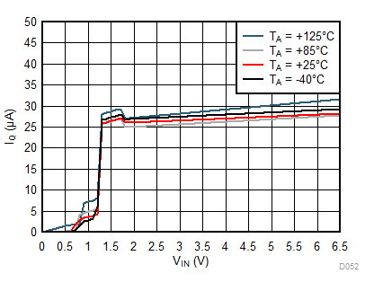
| IOUT = 0 mA |
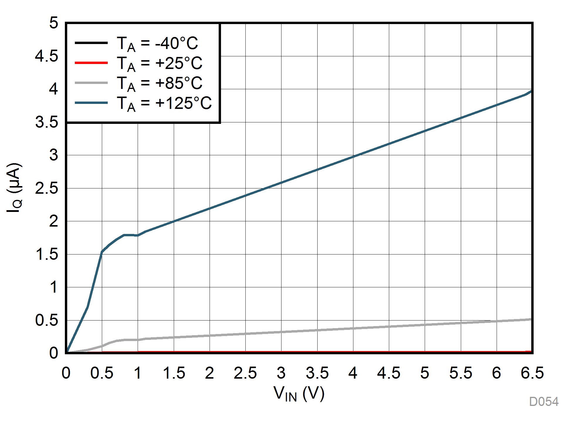
| VEN = 0 V |

| VEN = 0 V |
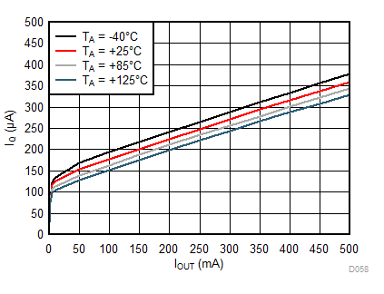
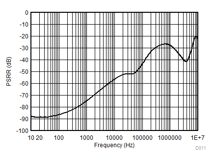
| VIN = 1.6 V | IOUT = 20 mA | |
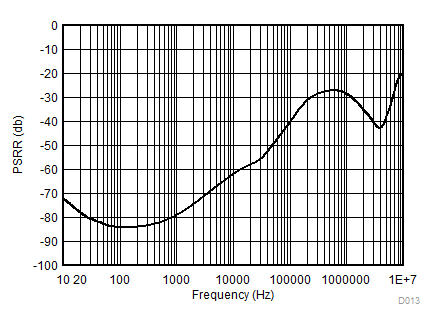
| IOUT = 20 mA | ||
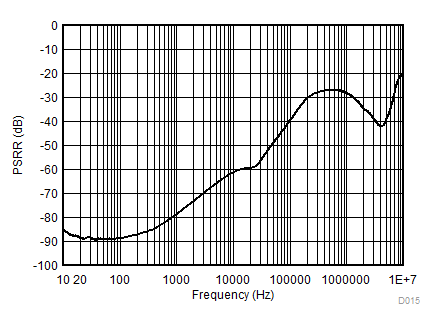
| IOUT = 20 mA | ||
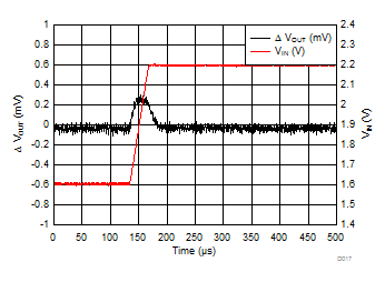
| VIN = 1.6 V to 2.2 V | trise = 30 µs | |
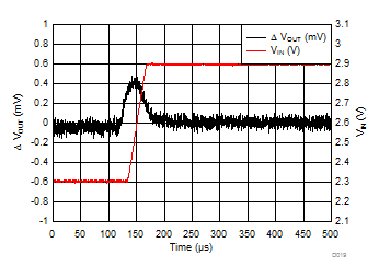
| VIN = 2.3 V to 2.9 V | trise = 30 µs | |
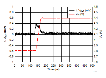
| VIN = 3.8 V to 4.4 V | trise = 30 µs | |
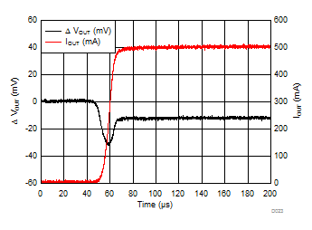
| VIN = 1.6 V | IOUT = 5 mA to 500 mA | trise = 10 µs |
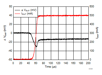
| IOUT = 5 mA to 500 mA | trise = 10 µs | |
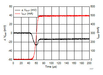
| IOUT = 5 mA to 500 mA | trise = 10 µs | |
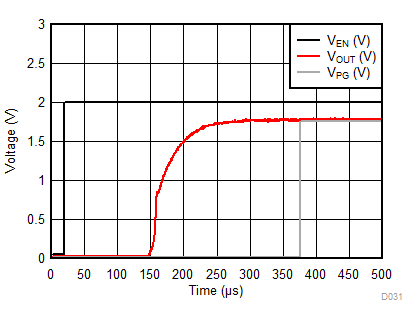
| IOUT = 0 mA | COUT = 1 µF | |

| IOUT = 1 mA | COUT = 1 µF |

| IOUT = 500 mA | COUT = 1 µF |
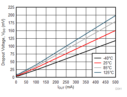
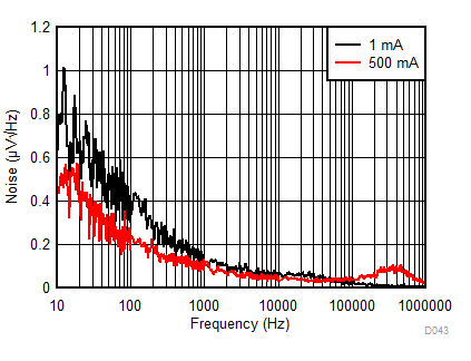
| VIN = 1.6 V |
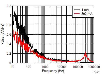
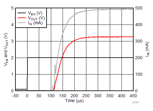
| CIN = Open | IOUT = 500 mA | COUT = 1 µF |
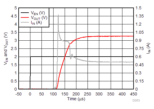
| CIN = Open | IOUT = 500 mA | COUT = 10 µF |