ZHCSFP8C December   2015  – September 2016 LP5912-Q1

PRODUCTION DATA.  

  1. 特性
  2. 应用
  3. 说明
  4. 修订历史记录
  5. Voltage Options
  6. Pin Configuration and Functions
  7. Specifications
    1. 7.1 Absolute Maximum Ratings
    2. 7.2 ESD Ratings
    3. 7.3 Recommended Operating Conditions
    4. 7.4 Thermal Information
    5. 7.5 Electrical Characteristics
    6. 7.6 Output and Input Capacitors
    7. 7.7 Typical Characteristics
  8. Detailed Description
    1. 8.1 Overview
    2. 8.2 Functional Block Diagram
    3. 8.3 Feature Description
      1. 8.3.1 Enable (EN)
      2. 8.3.2 Output Automatic Discharge (RAD)
      3. 8.3.3 Reverse Current Protection (IRO)
      4. 8.3.4 Internal Current Limit (ISC)
      5. 8.3.5 Thermal Overload Protection (TSD)
      6. 8.3.6 Power-Good Output (PG)
    4. 8.4 Device Functional Modes
      1. 8.4.1 Enable (EN)
      2. 8.4.2 Minimum Operating Input Voltage (VIN)
  9. Applications and Implementation
    1. 9.1 Application Information
    2. 9.2 Typical Application
      1. 9.2.1 Design Requirements
      2. 9.2.2 Detailed Design Procedure
        1. 9.2.2.1 External Capacitors
        2. 9.2.2.2 Input Capacitor
        3. 9.2.2.3 Output Capacitor
        4. 9.2.2.4 Capacitor Characteristics
        5. 9.2.2.5 Remote Capacitor Operation
        6. 9.2.2.6 Power Dissipation
        7. 9.2.2.7 Estimating Junction Temperature
      3. 9.2.3 Application Curves
  10. 10Power Supply Recommendations
  11. 11Layout
    1. 11.1 Layout Guidelines
    2. 11.2 Layout Example
  12. 12器件和文档支持
    1. 12.1 相关文档 
    2. 12.2 接收文档更新通知
    3. 12.3 社区资源
    4. 12.4 商标
    5. 12.5 静电放电警告
    6. 12.6 Glossary
  13. 13机械、封装和可订购信息

Pin Configuration and Functions

DRV Package
6-Pin WSON With Thermal Pad
Top View
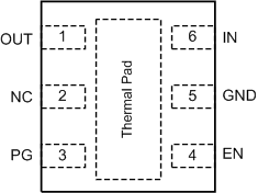
LP5912-Q1 pinout_snvsa77.gif

Pin Functions

PIN I/O DESCRIPTION
NUMBER NAME
1 OUT O Regulated output voltage
2 NC No internal connection. Leave open, or connect to ground.
3 PG O Power-good indicator. Requires external pullup.
4 EN I Enable input. Logic high = device is ON, logic low = device is OFF, with internal 3-MΩ pulldown.
5 GND G Ground
6 IN I Unregulated input voltage
Exposed thermal pad Connect to copper area under the package to improve thermal performance. The use of thermal vias to transfer heat to inner layers of the PCB is recommended. Connect the thermal pad to ground, or leave floating. Do not connect the thermal pad to any potential other than ground.