-
TPS40170 4.5V 至 60V 宽输入同步 PWM 降压控制器
- 1
- 1 特性
- 2 应用
- 3 说明
- 4 Pin Configuration and Functions
- 5 Specifications
-
6 Detailed Description
- 6.1 Overview
- 6.2 Functional Block Diagram
- 6.3
Feature Description
- 6.3.1 LDO Linear Regulators and Enable
- 6.3.2 Input Undervoltage Lockout (UVLO)
- 6.3.3 Oscillator and Voltage Feed-Forward
- 6.3.4 Overcurrent Protection and Short-Circuit Protection (OCP and SCP)
- 6.3.5 Soft-Start and Fault-Logic
- 6.3.6 Overtemperature Fault
- 6.3.7 Tracking
- 6.3.8 Adaptive Drivers
- 6.3.9 Start-Up into Pre-Biased Output
- 6.3.10 Power Good (PGOOD)
- 6.3.11 PGND and AGND
- 6.4 Device Functional Modes
-
7 Application and Implementation
- 7.1 Application Information
- 7.2
Typical Application
- 7.2.1 Design Requirements
- 7.2.2
Detailed Design Procedure
- 7.2.2.1 Custom Design with WEBENCH® Tools
- 7.2.2.2 List of Materials
- 7.2.2.3 Select a Switching Frequency
- 7.2.2.4 Inductor Selection (L1)
- 7.2.2.5 Output Capacitor Selection (C9)
- 7.2.2.6 Peak Current Rating of Inductor
- 7.2.2.7 Input Capacitor Selection (C1, C6)
- 7.2.2.8 MOSFET Switch Selection (Q1, Q2)
- 7.2.2.9 Timing Resistor (R7)
- 7.2.2.10 UVLO Programming Resistors (R2, R6)
- 7.2.2.11 Boot-Strap Capacitor (C7)
- 7.2.2.12 VIN Bypass Capacitor (C18)
- 7.2.2.13 VBP Bypass Capacitor (C19)
- 7.2.2.14 VDD Bypass Capacitor (C16)
- 7.2.2.15 SS Timing Capacitor (C15)
- 7.2.2.16 ILIM Resistor (R9, C17)
- 7.2.2.17 SCP Multiplier Selection (R5)
- 7.2.2.18 Feedback Divider (R10, R11)
- 7.2.2.19 Compensation: (R4, R13, C13, C14, C21)
- 7.2.3 Application Curves
- 7.3 Power Supply Recommendations
- 7.4 Layout
- 8 Device and Documentation Support
- 9 Revision History
- 10Mechanical, Packaging, and Orderable Information
- 重要声明
Data Sheet
TPS40170 4.5V 至 60V 宽输入同步 PWM 降压控制器
本资源的原文使用英文撰写。 为方便起见,TI 提供了译文;由于翻译过程中可能使用了自动化工具,TI 不保证译文的准确性。 为确认准确性,请务必访问 ti.com 参考最新的英文版本(控制文档)。
1 特性
- 可提供新款类似产品:
- 宽输入电压范围:4.5V 至 60V
- 600mV 基准电压,精度为 1%
- 可编程 UVLO 与迟滞功能
- 具有电压前馈的电压模式控制
- 可编程频率范围:100kHz 至 600kHz
- 可通过主要或辅助选项实现双向频率同步
- 提供基于低侧 FET 检测的过流保护与基于高侧 FET 检测的短路保护,具有集成式热补偿功能
- 可编程闭环软启动
- 支持预偏置输出
- 165°C 热关断,具有迟滞功能
- 电压跟踪
- 电源正常状态指示
- ENABLE 支持 1µA 低电流关断
- 提供 8.0V 和 3.3V LDO 输出
- 集成自举二极管
- 20 引脚 3.5mm × 4.5mm VQFN (RGY) 封装
- 使用 WEBENCH® 工具创建定制设计
2 应用
- POL 模块
- 适用于工业、网络以及电信设备的宽输入电压、高功率密度直流/直流转换器
3 说明
TPS40170 是一款功能齐全的同步 PWM 降压控制器,工作输入电压介于 4.5V 至 60V 之间,并针对高功率密度、高可靠性的直流/直流转换器应用进行了优化。该控制器通过输入电压前馈补偿实现电压模式控制,可在输入电压变化时即时响应。此器件具有 100kHz 至 600kHz 的可编程开关频率。
TPS40170 具有整套系统保护和监控特性,例如可编程欠压锁定 (UVLO)、通过检测低侧 FET 实现的可编程过流保护 (OCP)、通过检测高侧 FET 实现的可选短路保护 (SCP) 和热关断。通过 ENABLE 引脚,系统能够在低电流(典型值 1µA)模式下进行关断。控制器支持预偏置输出,提供开漏电源正常 (PGOOD) 信号,并具有闭环软启动、输出电压跟踪以及自适应死区时间控制功能。
TPS40170 可通过 1% 确保精度实现准确的输出电压调节。此外,该控制器还采用新型双向同步方案,即一个控制器作为主要控制器,其他下游控制器作为辅助控制器,辅助控制器可与主要控制器同相或 180° 异相同步。辅助控制器可在自由运行开关频率的 ±30% 范围内与外部时钟同步。
新款产品(LM5145 和 LM5146)具有 BOM 成本低、效率高、设计尺寸小等诸多特性。
(1) 有关所有可选封装,请参阅 节 10。
(2) 封装尺寸(长 × 宽)为标称值,并包括引脚(如适用)。
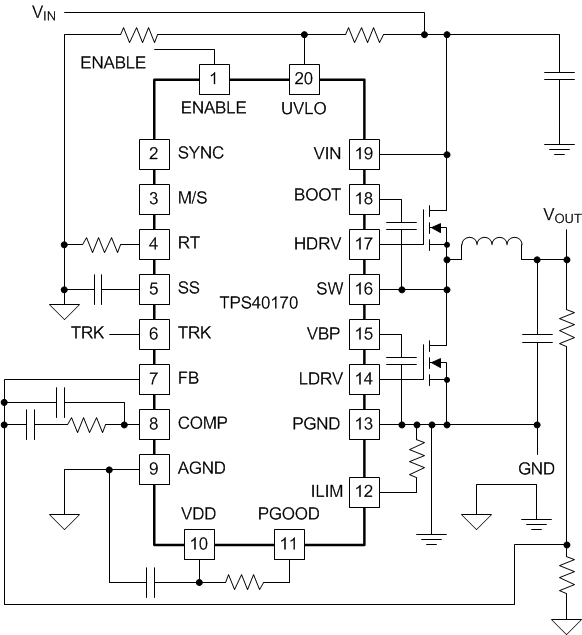
 简化版应用
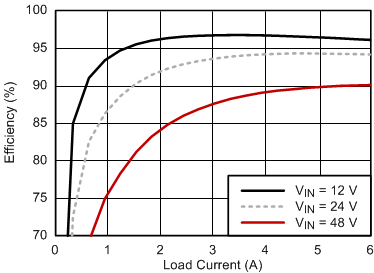
简化版应用 效率与负载电流之间的关系
4 Pin Configuration and Functions
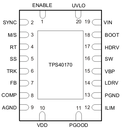
 Figure 4-1
RGY PACKAGE,
QFN-20
(Top View)
Table 4-1 Pin Functions
| PIN | TYPE(1) | DESCRIPTION | |
|---|---|---|---|
| NAME | NO. | ||
| AGND | 9 | — | Analog signal ground. This pin must be electrically connected to power ground PGND externally. |
| BOOT | 18 | O | Boot capacitor node for high-side FET gate driver. The boot capacitor is connected from this pin to SW. |
| COMP | 8 | O | Output of the internal error amplifier. The feedback loop compensation network is connected from this pin to the FB pin. |
| ENABLE | 1 | I | This pin must be high for the device to be enabled. If this pin is pulled low, the device is put in a low-power consumption shutdown mode. |
| FB | 7 | I | Negative input to the error amplifier. The output voltage is fed back to this pin through a resistor divider network. |
| HDRV | 17 | O | Gate driver output for the high-side FET. |
| ILIM | 12 | I | A resistor from this pin to PGND sets the overcurrent limit. This pin provides source current used for overcurrent protection threshold setting. |
| LDRV | 14 | O | Gate driver output for the low-side FET. Also, a resistor from this pin to PGND sets the multiplier factor to determine short-circuit current limit. If no resistor is present the multiplier defaults to 7 times the ILIM pin voltage. |
| M/S | 3 | I | Primary or secondary mode selector pin for frequency synchronization. This pin must be tied to VIN for primary mode. In the secondary mode this pin must be tied to AGND or left floating. If the pin is tied to AGND, the device synchronizes with a 180° phase shift. If the pin is left floating, the device synchronizes with a 0° phase shift. |
| PGND | 13 | — | Power ground. This pin must externally connect to the AGND at a single point. |
| PGOOD | 11 | O | Power good indicator. This pin is an open-drain output pin and a 10 kΩ pull-up resistor is recommended to be connected between this pin and VDD. |
| RT | 4 | I | A resistor from this pin to AGND sets the oscillator frequency. Even if operating in secondary mode, it is required to have a resistor at this pin to set the free running switching frequency. |
| SS | 5 | I | Soft-start. A capacitor must be connected at this pin to AGND. The capacitor value sets the soft-start time. |
| SW | 16 | I | This pin must connect to the switching node of the synchronous buck converter. The high-side and low-side FET current sensing are also done from this node. |
| SYNC | 2 | I/O | Synchronization. This is a bi-directional pin used for frequency synchronization. In the primary mode, it is the SYNC output pin. In the secondary mode, it is a SYNC input pin. If unused, this pin can be left open. |
| TRK | 6 | I | Tracking. External signal at this pin is used for output voltage tracking. This pin goes directly to the internal error amplifier as a positive reference. The lesser of the voltages between VTRK and the internal 600 mV reference sets the output voltage. If not used, this pin must be pulled up to VDD. |
| UVLO | 20 | I | Undervoltage lockout. A resistor divider on this pin from VIN to AGND can be used to set the UVLO threshold. |
| VBP | 15 | O | 8 V regulated output for gate driver. A ceramic capacitor with a value from 1 µF to 10 µF must be connected from this pin to PGND and placed close to this pin. |
| VDD | 10 | O | 3.3 V regulated output. A ceramic by-pass capacitor with a value from 0.1 µF to 1 µF must be connected from this pin to AGND and placed close to this pin. |
| VIN | 19 | I | Input voltage for the controller which is also the input voltage for the DC/DC converter. A ceramic by-pass capacitor with a value from 0.1 µF to 1 µF must be connected from this pin to PGND and placed close to this pin. |
(1) I = input, O = output