TIDUEB2A July 2022 – July 2022
- Description
- Resources
- Features
- Applications
- 5
- 1System Description
-
2System Overview
- 2.1 Block Diagram
- 2.2
Design Considerations
- 2.2.1 Power Multiplexing Circuit Design Parameters
- 2.2.2 Input Connections and Filter
- 2.2.3 Reverse Polarity Protection
- 2.2.4 Battery Charger Input
- 2.2.5 Battery Ideal Diode-OR
- 2.2.6 Input and Battery Switchover Mechanics
- 2.2.7 LM74800 (U1) HGATE
- 2.2.8 Battery LM74800 HGATE
- 2.2.9 BQ25731 Design Considerations
- 2.2.10 BQ25731 Component Selection
- 2.2.11 ILIM Circuit
- 2.2.12 MCU and I2C Bus Design Considerations
- 2.2.13 MSP430FR2475
- 2.2.14 I2C Bus Overview
- 2.2.15 MSP430 Connectors
- 2.2.16 MSP430 Power Supply
- 2.2.17 Sensing Circuits
- 2.2.18 Current Sensing
- 2.2.19 Voltage Sensing
- 2.2.20 Input Comparators
- 2.2.21 Software Flow Chart
- 2.3 Highlighted Products
- 3Hardware, Testing Requirements, and Test Results
- 4Design and Documentation Support
- 5Revision History
3.3.3 Circuit Switchover From Adapter to Battery
This test is designed to demonstrate the adapter-to-battery switchover capabilities of the design. The test is run with 19 V on the input supply. The E-Load is then connected to the system rail and draws a constant current of 8 A. The input supply is then removed and the VIN, VSYS, and VBAT rails are monitored for the switchover timings. The test is then repeated while replacing the 19-V input supply with a 13-V supply to mimic a car charging adapter.
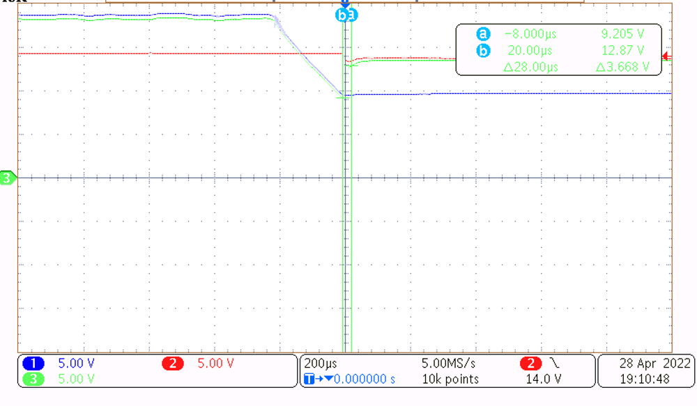
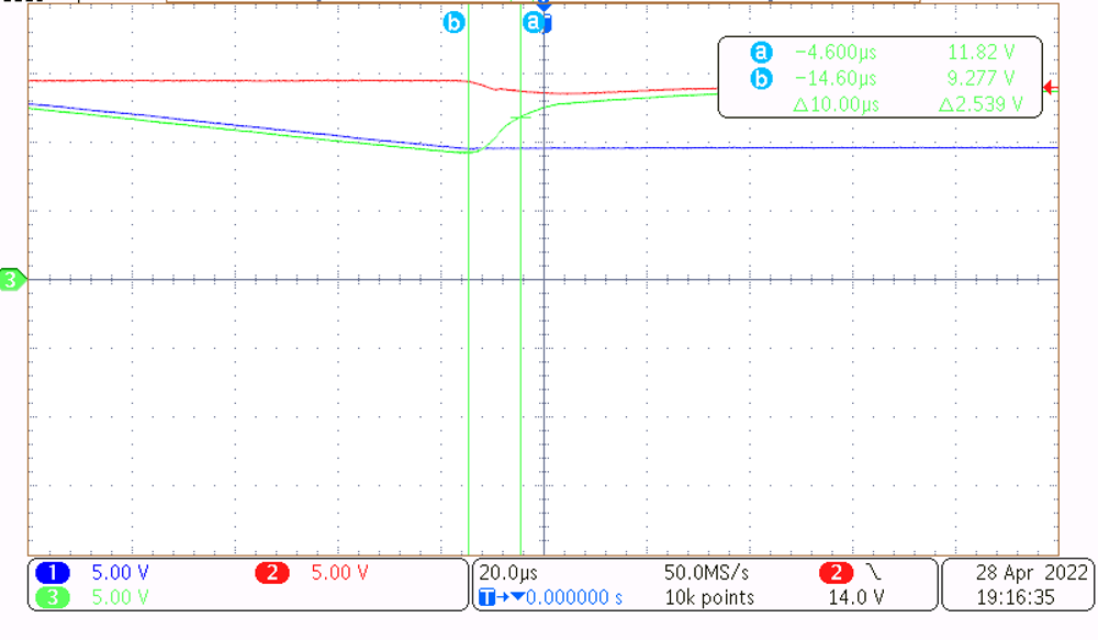
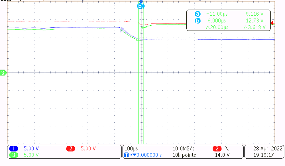
In Figure 3-1 through Figure 3-4, VIN is measured by CH1 (Blue), VBAT is measured by CH2 (Red) and, VSYS is measured by CH3 (Green). For these captures all channels are based at 0 V with no offset to better illustrate the switchover mechanism.
Figure 3-1 shows the 19 V to battery switchover with a time division of 200 μs. The minimum voltage at VSYS is 9.21 V. The approximate switchover timing is 10 μs and the VSYS rail has increased to 12.87 V by 20 μs after the switchover event.
 Figure 3-1 19 V to Battery Switchover
200-μs Time Division
Figure 3-1 19 V to Battery Switchover
200-μs Time DivisionFigure 3-2 shows the 19 V to battery switchover with a time division of 20 μs. The minimum voltage at VSYS is 9.28 V. The approximate switchover timing is 10 μs and the VSYS rail has increased to 11.82 V by 10 μs after the switchover event.
 Figure 3-2 19 V to Battery Switchover
20-μs Time Division
Figure 3-2 19 V to Battery Switchover
20-μs Time DivisionFigure 3-3 shows the 12 V to battery switchover with a time division of 100 μs. The minimum voltage at VSYS is 9.12 V. The approximate switchover timing is 10 μs and the VSYS rail has increased to 12.73 V by 20 μs after the switchover event.
 Figure 3-3 12 V to Battery Switchover
10-μs Time Division
Figure 3-3 12 V to Battery Switchover
10-μs Time DivisionFigure 3-4 shows the 12 V to battery switchover with a time division of 20 μs. The minimum voltage at VSYS is 9.31 V. The approximate switchover timing is 10 μs and the VSYS rail has increased to 10.63 V by 10 μs after the switchover event.
 Figure 3-4 12 V to Battery Switchover
20-μs Time Division