TIDT324 February 2023
2.4 Dimensions
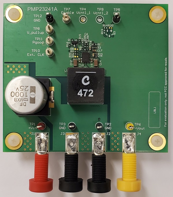
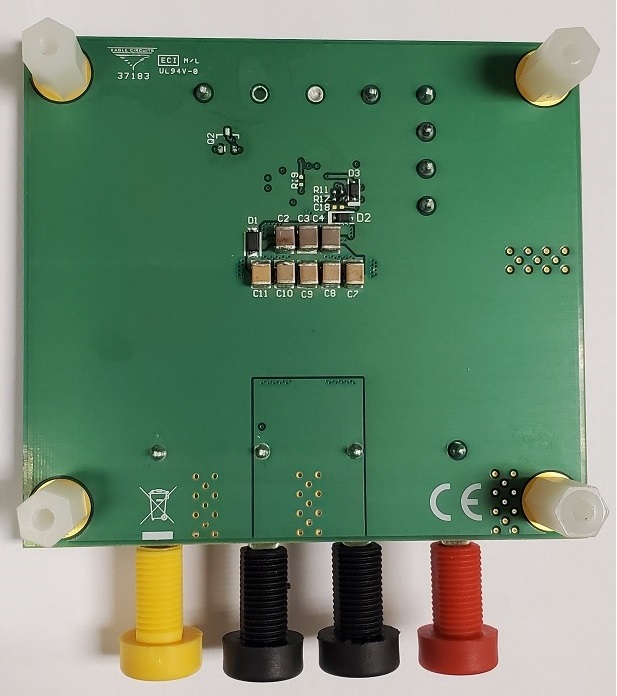
#FIG_PTX_LJM_JWB and #FIG_NSM_NJM_JWB show the top and bottom photos of the PMP23333 design which is built on the PMP23241A PCB. This board is a 4-layer board with 1-oz copper for each of the four layers. The board dimensions are 3.0 in × 2.7 in (76.2 mm × 68.58 mm). The actual design is approximately 0.67 in × 1.2 in (17.02 mm × 30.48 mm), excluding the input bulk capacitor, C1.
 Figure 2-4 Top of PMP23333
Board
 Figure 2-5 Bottom of PMP23333
Board