TIDT312 February 2023
3.1 Switching
Switching behavior is shown in the following figures.
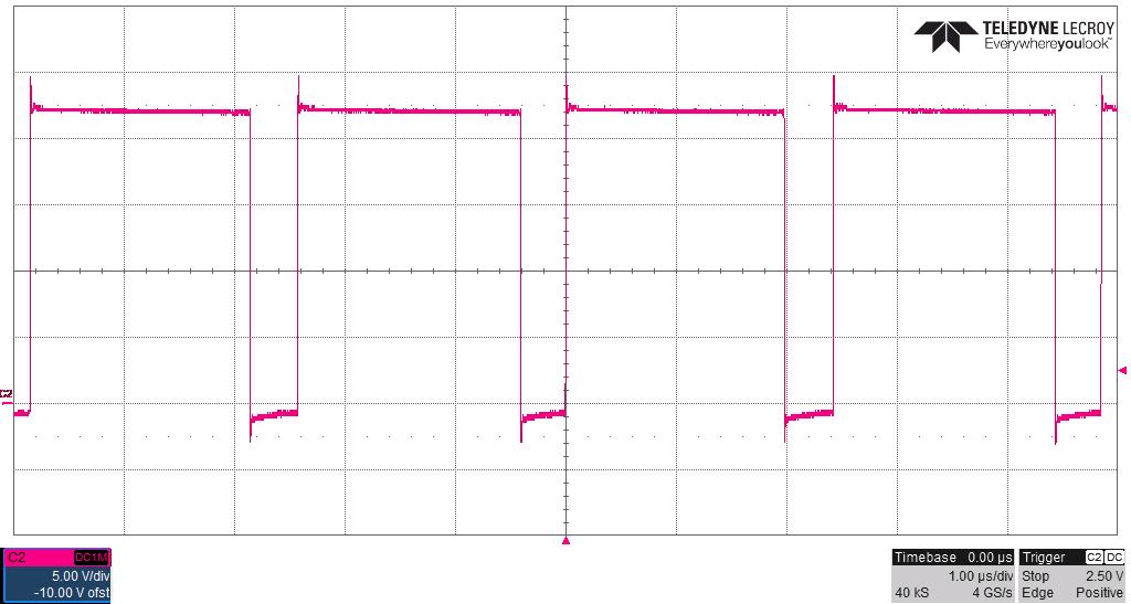 Figure 3-1 Primary FET Vds (U1 Pin 8) – 21.6
VIN, Full Load
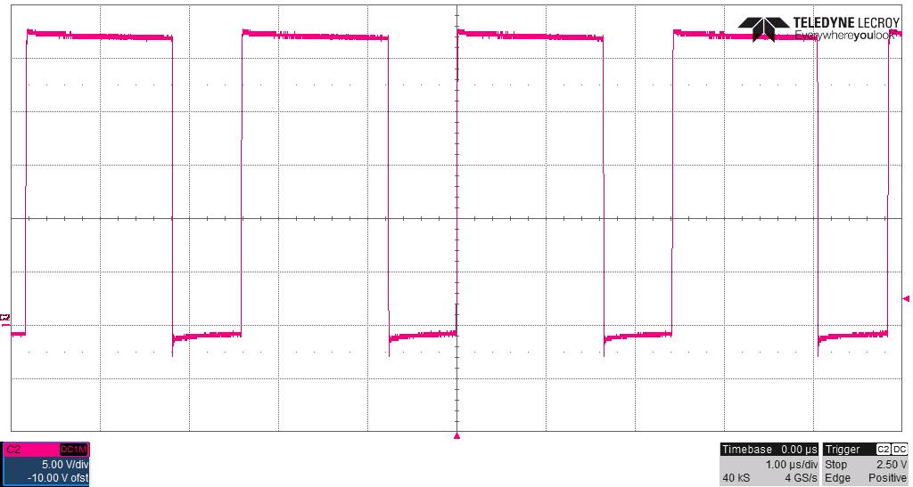 Figure 3-2 Primary FET Vds (U1 Pin 8) – 26.4
VIN, Full Load
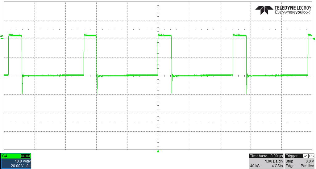 Figure 3-3 Diode (D4) – 21.6 VIN, Full Load
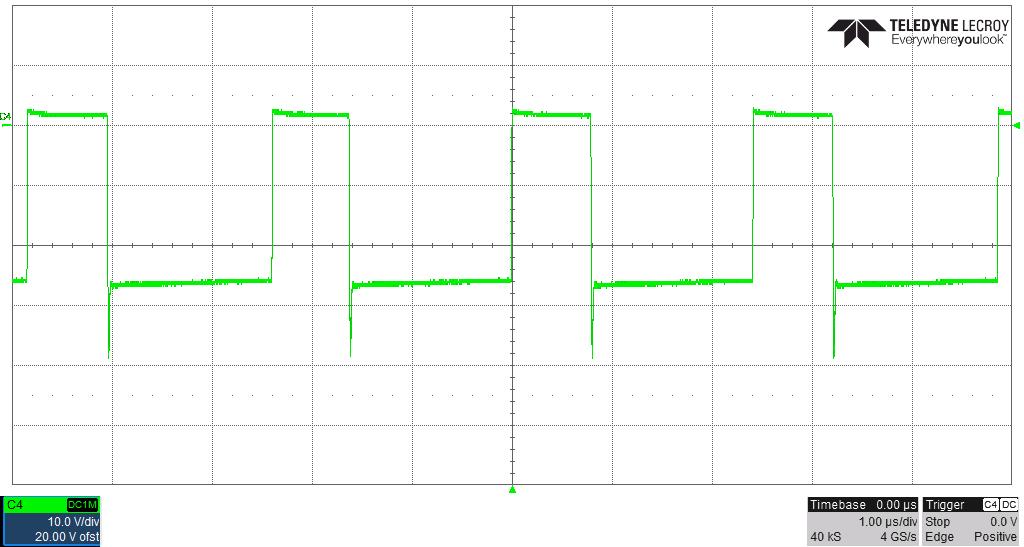 Figure 3-4 Diode (D4) – 26.4 VIN, Full Load
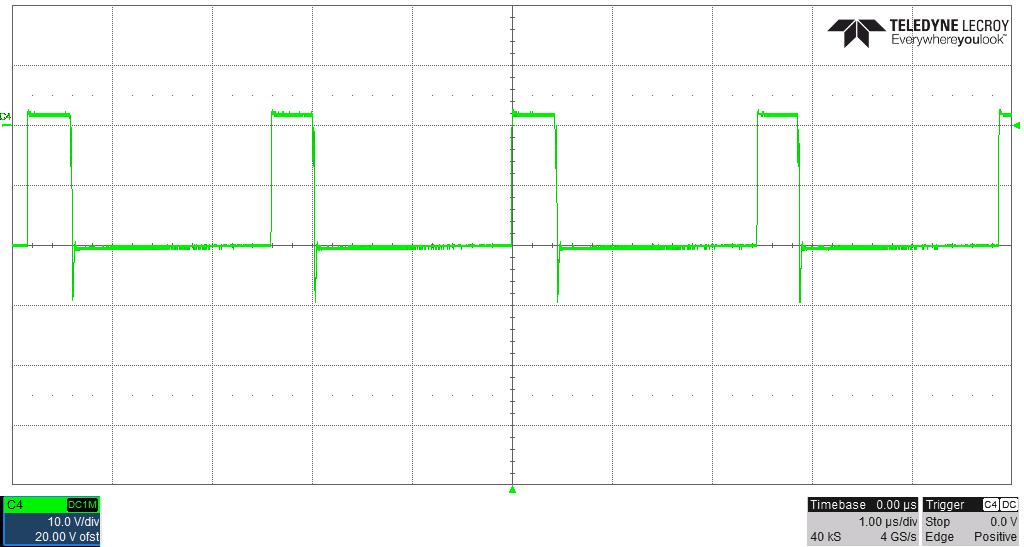 Figure 3-5 Diode (D2) – 21.6 VIN, Full Load
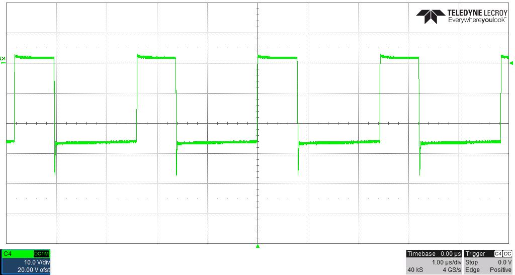 Figure 3-6 Diode (D2) – 26.4 VIN, Full Load