TIDT283 May 2022
2.4 Analog Sense
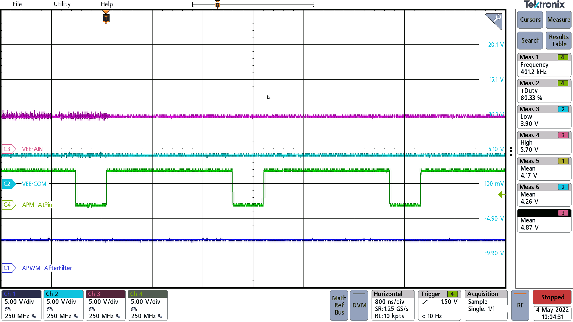
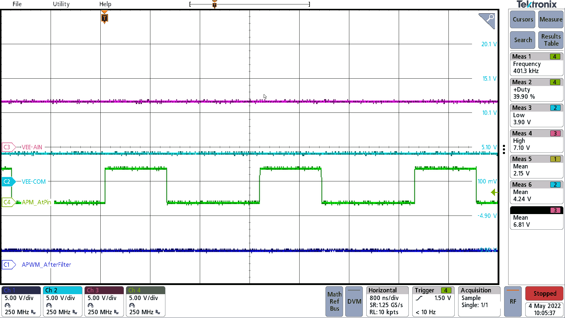
The analog sense feature of the UCC21732 is designed to allow easy temperature sensing across the isolation barrier, as described in the Isolated Analog to PWM Signal Function section of the UCC21732-Q1 10-A Source/Sink Reinforced Isolated Single Channel Gate Driver for SiC/IGBT with Active Protection, Isolated Analog Sensing and High-CMTI data sheet. The AIN voltage range is 0.6 V to 4.5 V, producing a PWM output on the APWM pin ranging from 88% duty cycle to 10% duty cycle. Figure 2-8 shows an AIN voltage of 4.87 V from VEE-AIN, which is 0.6 V from COM-AIN (Purple). The output PWM is 80.33% duty cycle (Green), and a filtered version of the APWM signal is 4.17 V which is an averaged version of the PWM output. Figure 2-9 shows the same waveforms, but with an input of 2.5 V to AIN, and a 40% APWM duty cycle. To use the APWM for power switch temperature sense connect a thermistor across J5. For more information, see the UCC21732-Q1 data sheet.
 Figure 2-8 Analog Sense With 0.6-V
AIN
 Figure 2-9 Analog Sense With 2.5-V AIN