TIDT235 April   2021


  1. 1Description
  2. 2Test Prerequisites
    1. 2.1 Voltage and Current Requirements
    2. 2.2 Required Equipment
    3. 2.3 Dimensions
  3. 3Testing and Results
    1. 3.1 Efficiency Graphs
    2. 3.2 Efficiency Data
    3. 3.3 Thermal Images
    4. 3.4 Load Regulation
  4. 4Waveforms
    1. 4.1 Switching
    2. 4.2 Output Voltage Ripple
    3. 4.3 Load Transients
    4. 4.4 Start-up Sequence

Switching

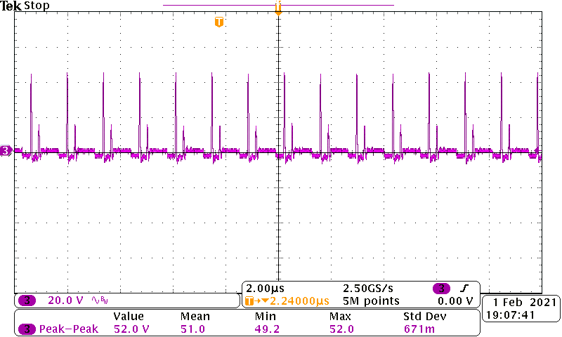
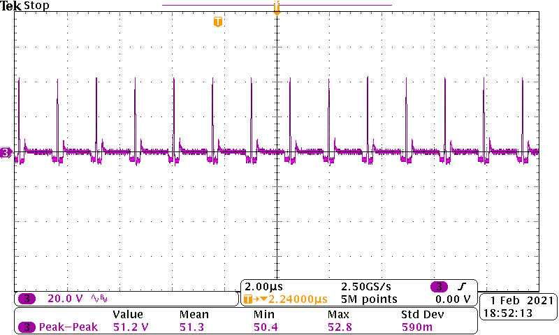
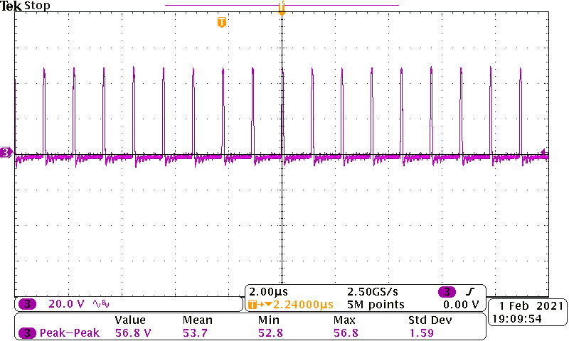
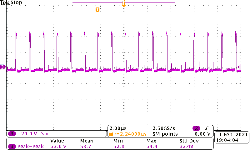
Switching behavior of the TPS61391 is shown in the following figures.
GUID-20210222-CA0I-X3CN-BCTN-VFZR3V9DZ6SK-low.png
CH3: VSW
Figure 4-1 3.3-V input, 48-V no load
GUID-20210222-CA0I-S8DX-35HD-VQ8LN6S5DSFV-low.png
CH3: VSW
Figure 4-3 5-V Input, 48-V no Load
GUID-20210222-CA0I-6HRC-FDFD-BGSRGLKJFFNZ-low.png
CH3: VSW
Figure 4-2 3.3-V Input, 48-V, 10-mA Load
GUID-20210222-CA0I-FP6Z-RR32-QVCR86F02MXB-low.png
CH3: VSW
Figure 4-4 5-V Input, 48-V, 20-mA Load