TIDT235 April   2021


  1. 1Description
  2. 2Test Prerequisites
    1. 2.1 Voltage and Current Requirements
    2. 2.2 Required Equipment
    3. 2.3 Dimensions
  3. 3Testing and Results
    1. 3.1 Efficiency Graphs
    2. 3.2 Efficiency Data
    3. 3.3 Thermal Images
    4. 3.4 Load Regulation
  4. 4Waveforms
    1. 4.1 Switching
    2. 4.2 Output Voltage Ripple
    3. 4.3 Load Transients
    4. 4.4 Start-up Sequence

Output Voltage Ripple

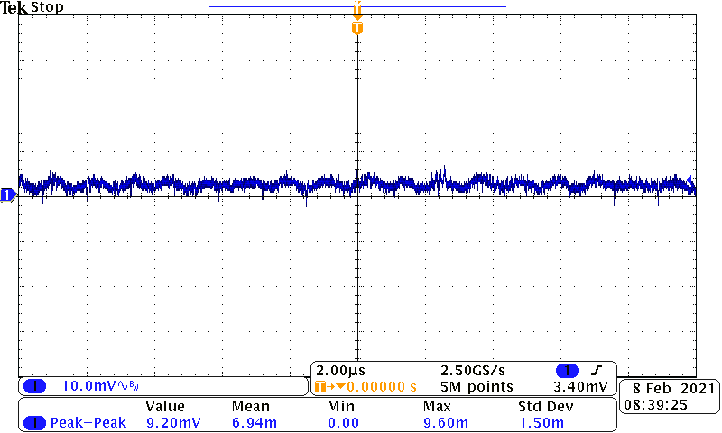
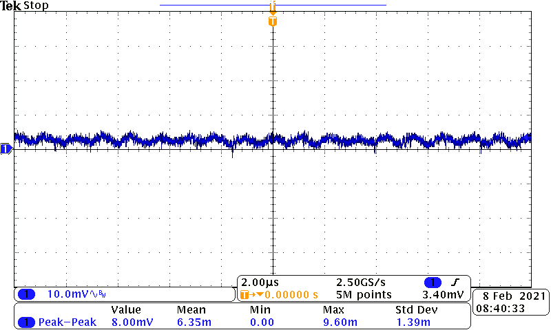
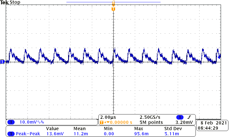
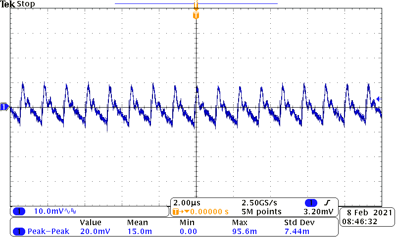
The output voltage ripple of the TPS61391 is shown in the following figures. It is also the input voltage ripple of the TPS7A4101.
GUID-20210222-CA0I-BXDR-Z51J-VQ7TDV7275FQ-low.png
CH1: VOUT(Boost)
Figure 4-5 3.3-V Input, 48-V no Load
GUID-20210222-CA0I-KDDJ-MRLV-B28RCMJJFBHN-low.png
CH1: VOUT(Boost)
Figure 4-7 5-V Input, 48-V no Load
GUID-20210222-CA0I-FP06-SKGJ-8S5NRT3S3GQV-low.png
CH1: VOUT(Boost)
Figure 4-6 3.3-V Input, 48-V, 10-mA Load
GUID-20210222-CA0I-KWP0-JPHM-K9QWK1HWLP2R-low.png
CH1: VOUT(Boost)
Figure 4-8 5-V Input, 48-V, 20-mA Load

The output voltage ripple of the LDO is shown in the following figures.
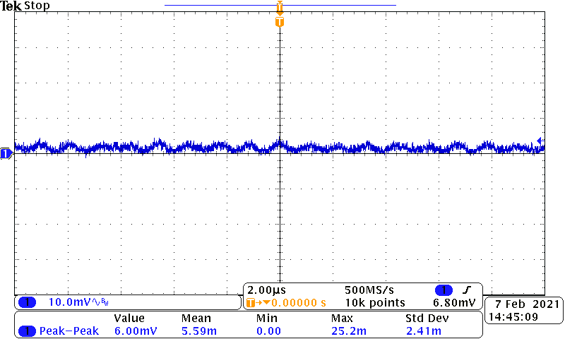
GUID-20210222-CA0I-HMQX-CVDK-XZTHRG0QDDZN-low.png
CH1: VOUT
Figure 4-9 3.3-V Input, 48-V no Load
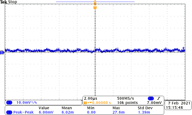
GUID-20210222-CA0I-F86G-DRLL-S09LCN4SJKL1-low.png
CH1: VOUT(Boost)
Figure 4-11 5-V Input, 48-V no Load
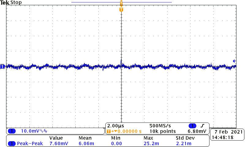
GUID-20210222-CA0I-PRRD-LVDK-LC5QNJL0WBKV-low.png
CH1: VOUT
Figure 4-10 3.3-V Input, 48-V, 10-mA Load
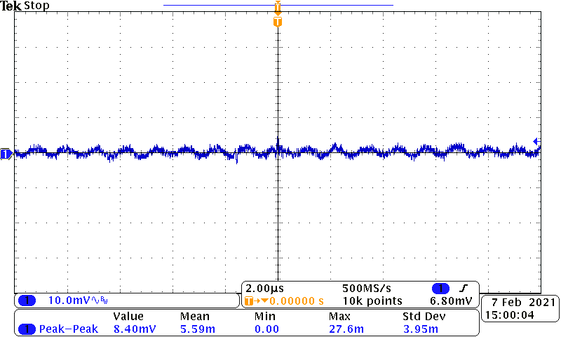
GUID-20210222-CA0I-QV40-TGD6-CGXQTZXZJG0G-low.png
CH1: VOUT(Boost)
Figure 4-12 5-V Input, 48-V, 20-mA Load