SSZTCS7 april 2015 CSD18502KCS
When it comes to MOSFET datasheets, you have to know what you’re looking for. While certain parameters are obvious and explicit (BVDSS, RDS(ON), gate charge), others can be ambiguous at best (ID, SOA curves), while others can be downright useless at times (see: switching times). In this series of blog posts, we will attempt to demystify the MOSFET datasheet, so that a reader can easily locate and discern the most usual data for their application, without getting bogged down by superfluous information or worse yet tricked by the games different vendors play to make their devices look more appealing on paper. If you are a more visual learner, you can follow this series in video format here.
Understanding MOSFET Data Sheets, Part 1 - UIS/avalanche Ratings
The unclamped inductive switching (UIS) rating has proven to be a useful parameter since becoming prevalent in MOSFET data sheets in the mid-1980s. While repetitive avalanching of the FET is not recommended in actual applications, engineers have learned to use this metric to avoid designing-in weaker devices that might cause issues. Devices with particularly weak UIS capability or heavy degradation over temperature (>30 percent from 25°C to 125°C) should raise a red flag, as these devices will be more susceptible to failing. Designers should also be weary of manufacturers playing games with the ratings to exaggerate their FET’s avalanche capability.
UIS testing is conducted with a test circuit like the one seen in Figure 1. A supply voltage is applied across the FET while it is turned off and the device is checked for leakage. As the FET is turned on, the inductor current steadily increases. When the desired current is achieved, the FET is switched off and the Ldi/dt voltage across the FET swings above the MOSFET’s breakdown, activating its intrinsic parasitic-bipolar transistor and effectively avalanching the FET. This test is repeated, ramping up the current incrementally, until destruction of the device occurs as evidenced by a failing of the preliminary leakage test.
 Figure 1 UIS Test Circuit
The equation E = ½ LI2 calculates the avalanche energy of the FET. This is where the games begin. By varying the inductor size, you can vary the stress placed on the device under test. Predictably, the larger the inductor, the lower UIS current required to destroy the FET. However, this smaller current is not offset by the increase of the inductor in the equation for avalanche energy such that this value actually increases even as the current decreases. Table 1 illustrates this relationship, which lists data gathered from testing TI’s CSD18502KCS 60V NexFET™ power MOSFET device.
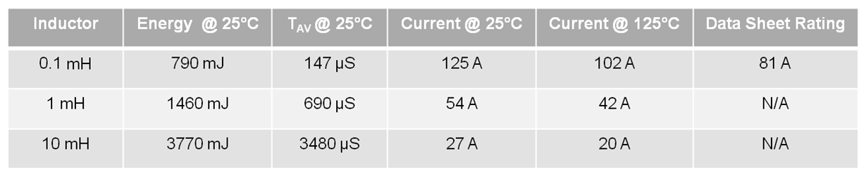
|
The most stressful, highest-current test occurs when using the smallest inductor (0.1mH) in the circuit. TI uses a 0.1mH inductor to test all devices going into production, and displays this associated energy value on FET data sheets. However, because there is no hard industry standard for this inductor value, some manufacturers will use a larger inductor in their UIS testing in order to give the appearance of higher avalanche-energy capability. Hence, designers need to approach avalanche ratings with caution, and make sure to inquire about the UIS test conditions before comparing FETs from different vendors.
In part two of “Understanding MOSFET data sheets,” I will address the safe operating area (SOA) graph that comes in all FET datasheets and give an example of how TI obtains the data used to generate this graph. In the meantime, watch a video "NexFET™:Lowest Rdson 80 and 100V TO-220 MOSFETs in the World" and consider one of TI’s NexFET power MOSFET products for your next design.