SSZTC82 september 2015 ADC3444 , TPS54120 , TPS54320 , TPS74701
In part 1 of this series, I demonstrated the impact of a DC/DC converter on the signal-to-noise ratio (SNR) and spurious-free dynamic range (SFDR) of a pipeline analog-to-digital converter (ADC). In part 2, I will use the analysis from my previous posts to implement a real-world power-supply solution that will minimize SNR and SFDR degradation while optimizing for solution size and efficiency.
In my “Noise requirements for ADC power supplies” post, I discussed the minimum thermal noise requirement of the power supply. I calculated that the maximum acceptable root mean square (RMS) noise value of 5µVRMS would not degrade the ADS3444 SNR of -73.9dB by more than 0.1dB or 20µVRMS, if a 0.9dB degradation was acceptable when considering the full Nyquist band.
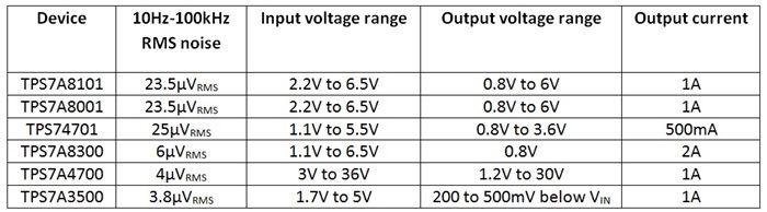
This leads to the LDO selections in Table 1.
|
I selected the TPS54120 DC/DC converter to generate the intermediate rail. Note that the TPS54120 is the integration of the TPS54320 DC/DC converter with the TPS7A8001 low-dropout regulator (LDO). As such, I will refer to the DC/DC converter by itself as the TPS54320 and the integrated solution as the TPS54120.
From a noise, power-supply rejection (PSR), output-current, cost and solution-size perspective, the best candidates are the TPS7A8001 and the TPS74701. The P-type metal-oxide semiconductor (PMOS) TPS7A8001 will have the best power-supply rejection ratio (PSRR) spec, while the TPS747 will have the lowest dropout voltage. These two solutions were driven by the TPS54120 DC/DC converter and will appear as TPS54320 + TPS747 and TPS54120 in Figure 1 through 7.
I evaluated the ADS3444 with a -2dBFS, 19.8MHz single-tone signal, disabling both chopper and dither.
 Figure 1 Complete Solutions
Developed
Figure 1 Complete Solutions
DevelopedThe solutions developed in Figure 1 use the LDO to provide the best PSR possible to the ADC. In order to use a single LDO, I inserted ferrite beads to minimize crosstalk between the DVDD and AVDD supplies. Figure 2 and Figure 3 show the block diagrams for the TPS54120 compact solution and the TPS54320 + TPS747 solution, respectively.
 Figure 2 TPS54120 Compact
Solution
Figure 2 TPS54120 Compact
Solution Figure 3 TPS54320 + TPS747
Solution
Figure 3 TPS54320 + TPS747
SolutionBoth solutions are very similar in their implementation. The main difference lies not in the LDO input or output voltage but in the type of LDO used. Both LDOs have similar noise, but differ in architecture and output-current capability. The TPS54120 LDO is a PMOS LDO with a 1A output-current capability, while the TPS747 is an N-type MOS (NMOS) LDO with a 500mA output-current drive. Although I did not implement it here, the TPS747 could operate with a much smaller dropout voltage than what I selected, potentially increasing overall solution efficiency.
Both solutions have good performance overall. In order to evaluate the PSR difference between the different solutions, I looked at the fast Fourier transform (FFT) result for both a no load (other than the ADC) and a 2A load, on top of the ADC current requirement. Only the DC/DC converter sees the additional load.
Figure 4 shows the FFT for the TPS54320 followed by the low-noise, 500mA TPS74701 LDO. I selected this LDO voltage regulator because it could achieve the lowest dropout voltage, thus minimizing system power consumption.
 Figure 4 TPS54320 + TPS747
Solution
Figure 4 TPS54320 + TPS747
SolutionFigure 5 shows the detail for the DC to 5MHz band and the band around the 19.8MHz tone.
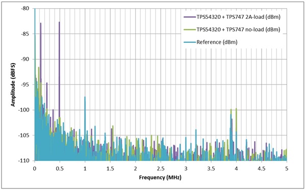
 Figure 5 TPS54320 + TPS747 Solution
Detail
Figure 5 TPS54320 + TPS747 Solution
DetailThe DC/DC converter driving the 2A load will degrade the ADC spur performance by approximately 5dB on most spurs and by 18dB at the DC/DC switching frequency. Now, looking at the higher performing and more compact TPS54120 solution, see Figure 6.
 Figure 6 Compact TPS54120
Solution
Figure 6 Compact TPS54120
SolutionThe 2A load has less degradation than the previous solution at the DC to 5MHz frequency band and the band around the 19.8MHz signal; see Figure 7.
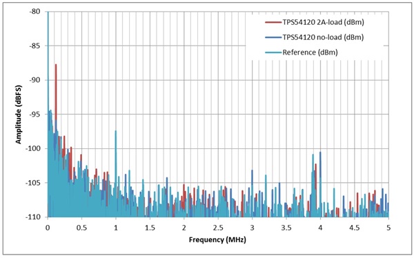
 Figure 7 Compact TPS54120 Solution
Details
Figure 7 Compact TPS54120 Solution
DetailsIn this series, I explained how to measure the PSR of an ADC, going through both thermal and switching-noise issues of the DC/DC converters and LDO, to post-filtering strategies, and finally designing the full solution and verifying its performance against an almost noiseless battery-operated power-supply design.
The best solution here, if designing for a smaller PCB area, is certainly the TPS54120. If your priority is to achieve the best efficiency, I recommend developing the TPS54320 + TPS74701 solution a little further, albeit with some performance degradation. As always, understanding the minimum requirements for an entire system and reducing those requirements to a small set of characteristics for component selection is the most challenging.
Keep TI in mind for your next power-chain design, as we have both a comprehensive portfolio and system knowledge to help you solve your most challenging designs. Let us help you.
In case you missed any other posts in this series, read my other blogs on creating a power supply for ADCs.