SSZTA44 June 2017 TDA2SX
When we look back 20 years from now, automotive evolution will likely be considered the greatest in recent times. Future automotive evolution will be profoundly impacted by automating the task of driving. While there are many aspects to achieving safe and reliable semi-autonomous and fully autonomous driving, it’s clear it will require a “vision” system that is accurate, reliable and can fit into reasonable budgets as well. Multiple modalities, such as camera, ultrasonic, RADAR and LIDAR sensing, when fused together, can greatly increase the reliability of resulting data used to determine a vehicle’s course of action. The processing of all these signal types is critical and ultimately needs to be accomplished within reasonable power, price and performance budgets that can support a safer, reliable and commercially viable solution.
Texas Instruments’ long history in signal processing and the automotive market drives advancement in the development of our automotive processors. To date, TI has shipped over 150 million units into this market. The experience gained by working with major customers to create automotive grade products for more than a decade has facilitated our development of a scalable, cost-effective family of devices offering our customers the best compute per watt solutions targeted for Advanced Driver Assist Systems (ADAS). These systems are the building blocks for near-term, semi-autonomous driving and safety functions as well as long-term, fully autonomous vehicles. Digital signal processing (DSP) is at the core of TI’s Driver Assist (TDAx) family and our extensive experience in this market has driven us to also implement on-chip accelerators of specialized functions found in key applications such as automated emergency braking, adaptive cruise control, lane keep assist, traffic sign recognition, surround viewing, self-parking and many others.
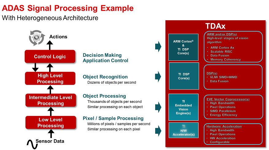
These efficient, DSP cores and optimized accelerators for critical functions are augmented by more general purpose ARM® cores for control code and high-level application software. As seen in Figure 1, the heterogeneous architecture of TI’s TDAx family of automotive processors maps extremely well to typical ADAS signal processing functions. Each of these tailored-fit, programmable cores and accelerators are connected by an extremely efficient internal bus fabric to help ensure the highest levels of overall functional utilization. This hardware architecture, along with TI’s Vision SDK, enables very effective solutions for ADAS applications. To learn more about the TDAx heterogeneous architecture, please refer to our corresponding white paper.
 Figure 1 TDAx Heterogeneous
Architecture
 Given the automotive market’s evolution toward broader and deeper ADAS functions, there is a very real need for scalable solutions to address the different price and performance points required for these various systems. The TDAx family offers this via its heterogeneous architecture (from a core multiplier and frequency perspective) that also enables software compatibility and extensibility. This provides an optimized fit for a specific ADAS system whether it is a forward vision system that includes both camera and radar sensing, a four-camera surround view system with self-parking, a camera mirror replacement system with blind spot detection, or other various types of ADAS systems. Building solutions on this scalable architecture saves time and money as well as promotes faster product development over time.
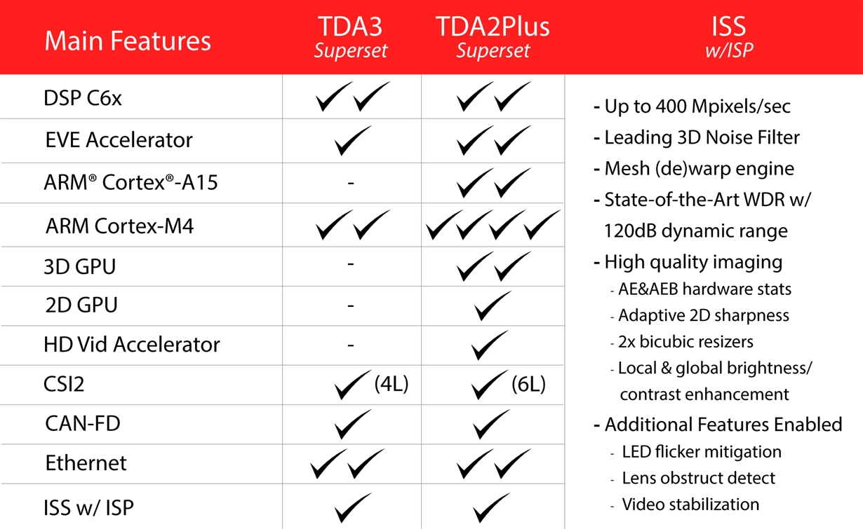
One of these aforementioned evolutions is the use of smaller-sized, cost-reduced camera modules that do not include an integrated image signal processor (ISP). The elimination of the in-module ISP not only helps reduce the camera size and cost, it also helps to significantly reduce the power consumption and resultant heat, which can be detrimental to the image quality captured by the sensor. Furthermore, these contemporary camera modules typically use a low voltage differential signaling (LVDS) interface instead of Ethernet to further help reduce size, cost and heat. The image data provided upstream is not compressed and is sent “raw” (no loss) for processing in the corresponding SoC, such as TDAx. This helps promote image quality and ultimately provide for a more reliable and potentially safer solution. To take advantage of this trend, both the current TDA3 and upcoming TDA2Plus families include an integrated sixth generation, high-quality ISP within their imaging subsystem (ISS) in addition to the other cores previously discussed.
 Figure 2 TDA3 and TDA2Plus Feature
Overview
Figure 2 TDA3 and TDA2Plus Feature
OverviewThis subsystem enables easier and higher quality exposure matching of the images as well as lens distortion correction. Other additional processing, such as LED flicker mitigation, can also be easily afforded given the architecture and available cores on these devices. Figure 2 provides an overview of TDA3 and TDA2Plus offerings with integrated ISS and some of its many features. To learn more about integrated ISS on TDA devices, please refer to our corresponding white paper. These image processing capabilities along with the TDAx DSP and EVE cores provide a very compelling solution for fusing multiple sensing modalities to create a more reliable and safer system. The TDAx family continues to evolve to address the trends within the automotive ADAS market and provides the best balanced and scalable solutions for enabling these functions across a family of vehicles.
The TDAx devices from Texas Instruments along with other supporting automotive grade components, such as PMICs and FPD-Link serializers/deserializers, can be found on http://www.ti.com.
Want to learn more? See below for related content you may be interested in: