SSZT976 august 2017 DS92LV0421 , DS92LV0422 , DS92LV2421 , DS92LV2422 , SN65LVDS047 , SN65LVDS388A , SN65LVDS389 , SN65LVDS822 , SN75LVDS83B
Multifunction and Industrial printers often include a data path where an image must be passed between multiple boards in the system. This creates concerns for designers including noise immunity, electromagnetic interference (EMI), and power consumption over these links. In this post, I’ll take a look at how the different circuit boards in multifunction and industrial printers communicate with each other, with a particular focus on where low-voltage differential signaling (LVDS) is applicable.
Multifunction printers integrate office document management functions into one device. These functions include the ability to email, fax, photocopy, print and scan. There are two types of industrial printers: large format printers, which support a print-roll width of over 18 inches for printing banners, circuit schematics, architectural drawings or other large-format materials; and production printers, which are used for high-speed, high-volume printing of manuals or booklets.
LVDS transmits image data within these printers (from the scanning elements, to a user interface screen, to the printing elements), in addition to transmitting clock and/or control data between boards in the system.
When compared to other communication methods, LVDS provides the following advantages:
- Noise immunity due to differential signaling.
- Longer communication distances due to current-mode logic.
- Low EMI due to having opposite signals on differential lines in a twisted-pair cable.
- Low power consumption.
Additionally, serialized LVDS signals provide these additional advantages over parallel LVDS:
- Reduced layers on the printed circuit board (PCB).
- Reduced cable weight and cost.
- Additional EMI reduction.
- No need to worry about skew among parallel lines and clock.
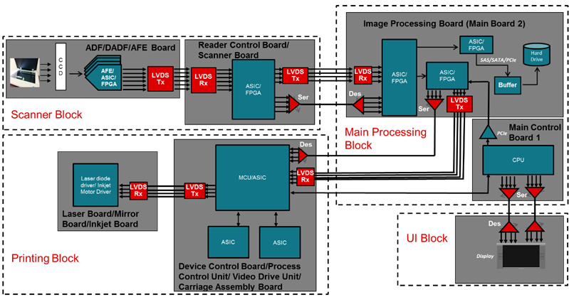
Figure 1 depicts a functional breakdown of a multifunction or industrial printer. Although LVDS functionality is increasingly integrated into field-programmable gate arrays (FPGAs) and application-specific integrated circuits (ASICs), for the purposes of this blog post, I’ll treat all LVDS functionality as discrete. A conceptual data path for a printer begins with a scanned image that passes to the main board for image processing. The image to be printed then passes to a printer control board. Let’s explore the signal chain for image data as it is scanned, manipulated and printed.
 Figure 1 Multifunction/Industrial Printer Simplified Block Diagram
The signal chain in a multifunction or industrial printer can be conceptualized into four blocks:
- Scanner block.
- Main processing block.
- Printing block.
- User interface block.
Scanner Block
Figure 2 takes a close look at the scanner block. This block receives image data from the charge-coupled device (CCD), usually through a dedicated analog front-end ASIC, and passes this data to the main processing unit. The scanner block may split into separate automatic document feeder (ADF) and reader control boards, as Figure 2 shows, or combined. Analog front-end ASICs transmit the scanned image data via parallel LVDS to the reader ASIC, or directly to the image processing board. If the design has a separate reader ASIC (as shown in Figure 2), parallel LVDS or SerDes LVDS is used to receive and transmit that image data to the image processing board. The cable length required between the reader control board and the image processing board can be the deciding factor in whether to use parallel or SerDes LVDS, as you can offset the extra cost and engineering work involved with implementing a SerDes solution by reduced cable cost and/or reduced EMI. TI’s DS92LV2421/DS92LV2422 and DS92LV0421/DS92LV0422 are good example of serializer/deserializer pairs to implement this functionality.
 Figure 2 Scanner Block Diagram
Main Processing Block
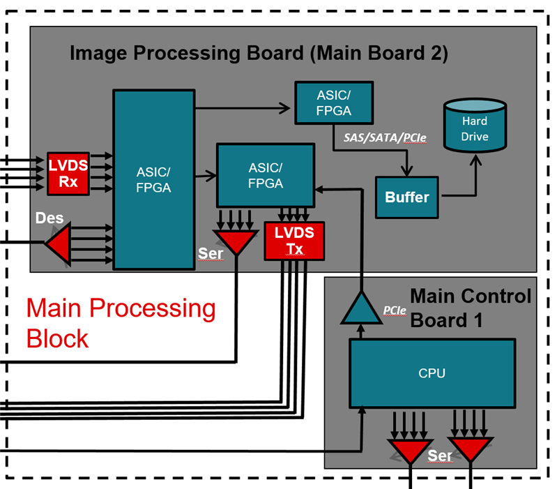
The main processing block consists of an image processing board and a main control board. The image processing board contains ASICs/FPGAs that receive the scanned image data sent from the scanner. If the printer is operating as a photocopier, the image data passed to the image processing board is manipulated and sent via LVDS to the printing block. If the image data comes from another source (email, cloud printing, etc.), the image processing board formats the data and passes it via LVDS to the printing block.
LVDS communication is also used to transmit image data for the user interface to a screen on the front of the printer from the central control board. These transmission distances might approach 2 feet of cable length, and occur via SerDes (shown at the bottom right of Figure 3). Multiple SerDes lanes may transmit this data, with data rates around 1.5Gbps depending on the resolution of the user interface screen.
 Figure 3 Main Processing Block Diagram
Printing Block
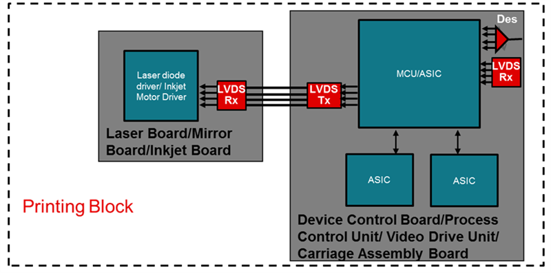
The printing block consists of a device control board and a laser board or inkjet board, depending on the print methods used. The device control board receives the image data to be printed (either via a deserializer or a parallel LVDS receiver) and performs additional functions to change the data into control signals for the laser board or inkjet board. The LVDS link between the device control board and the laser/inkjet board transmits these control signals, along with clock information. TI’s SN65LVDS389/SN65LVDS388A is an example of a transmitter/receiver pair well-suited for this application.
 Figure 4 Printing Block Diagram
User Interface Block
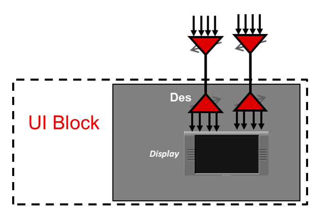
The user interface block consists of the display screen and any hardware needed to configure the signal for that display. Data sent via serialized LVDS will require a deserializer, and the output of that deserializer will depend on the input format required by the display (RGB or LVDS). TI’s SN75LVDS83B/SN65LVDS822 is an example of a serializer/deserializer pair that can transmit RGB levels through LVDS and translate back to RGB at the receiving end for a display.
 Figure 5 User Interface Block
In summary, LVDS is a preferred method of communication when transmitting high-speed data over longer distances or when there are concerns about EMI, power consumption or cable cost/PCB layer cost.
Leave a comment below if you want to learn more about anything discussed here, or if there is an LVDS topic you would like to see in the future.
Additional Resources
- Get online support in the TI E2E™ Community Interface forum.
- Learn more about TI’s portfolio of LVDS solutions.