SSZT928 october 2017 ADS8900B , LMS3655 , THS4551 , TPS7A30
When creating high-performance test and measurement equipment, the last thing on your mind is what is powering the board. It may be hard to believe, but the power supply can have a drastic impact on the performance of high-precision successive-approximation-register (SAR) analog-to-digital converters (ADCs) that are downstream to the power supply. Using an electromagnetic interference (EMI)-optimized power supply can be tremendously valuable for a number of different applications, including data-acquisition systems, semiconductor test equipment, spectrum analyzers and oscilloscopes.
By using a DC/DC switching buck converter optimized for EMI performance instead of a standard buck converter, you can achieve an improvement of as much as 2dB and 12dB for the signal-to-noise ratio (SNR) and spurious-free dynamic range (SFDR), respectively. For the analysis, I used two 20-bit SAR ADC (ADS8900B) channels, the THS4551 fully differential amplifier and the LM53635 EMI-optimized 36V buck converter followed by the TPS7A30 low-dropout regulator (LDO); see the Multi-Rail Power Reference Design for Eliminating EMI Effects in High Performance DAQ Systems.
There are three key developments in the LM53635 buck converter that lead to its excellent EMI performance:
- HotRod™ packaging.
- Symmetrical pinout enabling concentric current loops for the input capacitors.
- Spread-spectrum feature.
The LM53635 uses HotRod packaging, which is TI’s implementation of a flip-chip on-lead (FCOL) frame device. Instead of having a bond wire connecting the die to the lead frame, the die is flipped over and directly soldered to the lead frame; see Figure 1 and Figure 2. Removing the bond wire reduces the amount of parasitic inductance, which is a source of high-frequency noise that is difficult to filter out. Another benefit of HotRod packaging technology is that it reduces the drain-source on-resistance (RDS(on)) of the device, which actually improves device efficiency.
 Figure 1 Standard Wire-bond Quad
Flat No-lead (QFN) Device
 Figure 2 HotRod FCOL QFN
Device
Figure 2 HotRod FCOL QFN
DeviceFigure 3 shows the immediate benefit of the HotRod package in the switch node of the LM53635 buck converter.
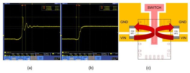 Figure 3 Switch node of standard buck
converter with bond wire (a); switch node of the EMI-optimized LM53635 with
HotRod packaging (b); symmetrical VIN/ground planes provide an
EMI-optimized pinout for the LM53635 (c)
Figure 3 Switch node of standard buck
converter with bond wire (a); switch node of the EMI-optimized LM53635 with
HotRod packaging (b); symmetrical VIN/ground planes provide an
EMI-optimized pinout for the LM53635 (c)While HotRod packaging improves EMI performance, another optimization is in the pinout of the device. The VIN/ground planes of the LM53635 are designed to be symmetrical, which enables you to place input capacitors in parallel and thus reduce the size of the input current loops. Putting this parasitic inductance in parallel also reduces ringing and helps mitigate high-frequency EMI.
Another great feature of the LM53635 is the spread-spectrum feature, which enhances EMI performance by dithering the frequency ±3% to help reduce the fundamental energy peaks. The spread-spectrum feature can reduce high-frequency peak emissions by up to 6dB and slightly less than 1dB at lower frequencies. With a 36VIN maximum operating voltage, the LM53635 is optimized for systems up to 18VIN and can efficiently convert that voltage down to 3.3VOUT at 2.1MHz. When the voltage exceeds 18V, the device will smoothly fold the frequency back from 2.1MHz.
Another device, the LMS3655, is a 400kHz version of the LM53635 and can efficiently convert a 24VIN down to 1VOUT without any frequency fold-back, since there will be no minimum on-time violations while switching at 400kHz. While the LM53635 offers a smaller solution in inductor and total solution size due to its 2.1MHz frequency, the LMS3655 is optimized for efficiency – with a peak efficiency of 96% with a 12VIN to 5VOUT conversion. Both the LM53635 and LMS3655 share the EMI performance-optimizing features.
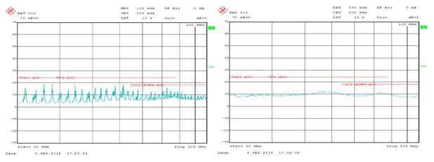 Figure 4 High-frequency-conducted EMI
Results (30-108MHz) without Spread Spectrum (Left) and with Spread Spectrum
(Right). the Red Lines Superimposed on the Graph Denote Limits from the
Stringent Comité International Spécial Des Perturbations Radioélectriques
(CISPR) 25 Class 5 Standard, with 28dB Limits from 30-54MHz and 18dB Limits from
70-108MHz.
Figure 4 High-frequency-conducted EMI
Results (30-108MHz) without Spread Spectrum (Left) and with Spread Spectrum
(Right). the Red Lines Superimposed on the Graph Denote Limits from the
Stringent Comité International Spécial Des Perturbations Radioélectriques
(CISPR) 25 Class 5 Standard, with 28dB Limits from 30-54MHz and 18dB Limits from
70-108MHz.TI tested the LM53635 in the exact same configuration as a similar buck converter not as optimized for EMI with a 24V input, with the output connected to the same LDOs, and tested the performance of the ADCs. The Performance of the LM53635 vs. a non-EMI Optimized Switching Buck Regulator in the Exact Same Configuration and Figure 6 and Figure 7 show the impact of the optimizations in the LM53635.
 Figure 5 The Performance of the LM53635
vs. a non-EMI Optimized Switching Buck Regulator in the Exact Same
Configuration
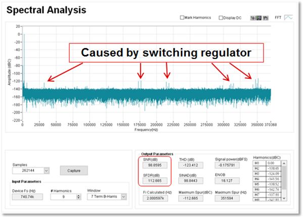 Figure 6 Spectral Analysis of a non-EMI
Optimized Buck Converter, Showing a Number of Spurs Spiking Out
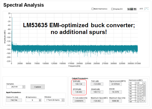 Figure 7 The LM53635 EMI-optimized Buck
Converter with No Additional Spurs (unlike Figure 6)
Figure 7 The LM53635 EMI-optimized Buck
Converter with No Additional Spurs (unlike Figure 6)You can easily see the performance enhancements of using the LM53635 buck converter for a high-precision application. Using this EMI-optimized device results in a +1dB gain in SNR and a +13dB gain in SFDR vs. a similar buck converter not optimized for EMI. While the power tree is not generally an area that most designers spend a lot of time on, choosing the right switching regulator can have a huge impact on the overall sensitivity of a system.
Additional Resources
- Watch the video, “Designing Low-EMI Power Converters for Industrial and Automotive Systems.”
- Check out the Reference Design Optimizing FPGA Utilization and Data Throughput for Automatic Test Equipment.
- Demonstrate optimized density and integration for your test equipment with our reference design