SSZT173 april 2021 LM25149-Q1 , LM5156-Q1 , LM62440-Q1
Electronic systems in industrial, automotive and personal computing applications are becoming increasingly dense and interconnected. To improve the form factor and functionality of these systems, diverse circuits are packed in close proximity. Under such constraints, reducing the effects of electromagnetic interference (EMI) becomes a critical system design consideration.
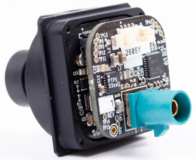
Figure 1 shows an example of such a multi-functional system, an automotive camera module, where a 2-megapixel imager is packed in close proximity with a 4-Gbps serializer and a four-channel power-management integrated circuit (PMIC). A byproduct of the ensuing increase in complexity and density is that sensitive circuitry like the imager and signal-processing elements sit very close to the PMIC, which carries large currents and voltages. This placement inevitably leads to a set of circuits electromagnetically interfering with the functionality of the sensitive elements – unless you pay careful attention during design.
 Figure 1 Automotive Camera
Module
Figure 1 Automotive Camera
ModuleElectromagnetic interference (EMI) can manifest itself in two ways. Consider the case of a radio connected to the same power supply as a motor drill, as shown in Figure 2. Here, the operation of the sensitive radio system is affected through conductive means by the motor, since they both share the same outlet for power. The motor also affects the functionality of the radio through electromagnetic radiation that couples over the air and is picked up by the radio’s antenna.
When end-equipment manufacturers integrate components from various sources, the only way to guarantee that interfering and sensitive circuits can coexist and operate correctly is through the establishment of a common set of rules that sets limits for the interfering circuits to be within and which the sensitive circuits need to be capable of handling.
 Figure 2 Electromagnetic interference
caused by conducted and radiated means
Figure 2 Electromagnetic interference
caused by conducted and radiated means| Learn more about time-saving and cost-effective innovations for EMI reduction in power supplies Read the white paper now |
Common EMI Standards
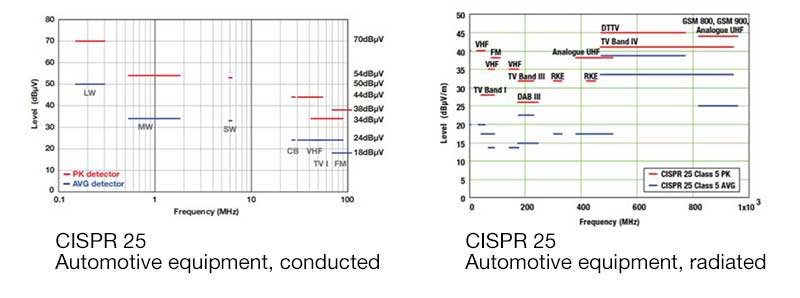
Rules designed to limit interference are established in industry-standard specifications such as Comité International Spécial des Perturbations Radioélectriques (CISPR) 25 for the automotive industry, and CISPR 32 for multimedia equipment. CISPR standards are critical for EMI designs, as they dictate the targeted performance of any EMI mitigation technique. CISPR standards are categorized into conducted and radiated limits depending on the mode of interference, as shown in Figure 3. The bars in the plots in Figure 3 represent the maximum conducted and radiated emission limits that the device under test can tolerate when measured using standard EMI measuring equipment.
 Figure 3 Typical standards for conducted and radiated EMI
Causes of EMI
Building systems compatible with EMI standards requires a clear understanding of the primary causes of EMI. One of the most common circuits in modern electronic systems is the switch-mode power supply (SMPS), which provides significant improvements in efficiency over linear regulators in most applications. But this efficiency comes at a price, as the switching of power field-effect transistors in the SMPS causes it to be a major source of EMI.
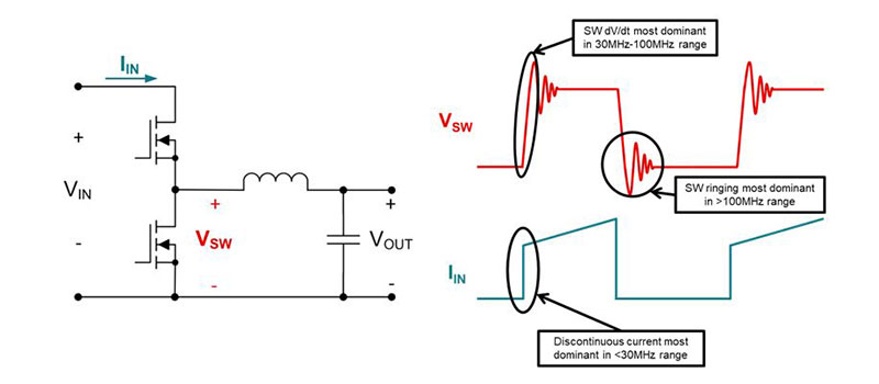
As shown in Figure 4, the nature of switching in the SMPS leads to discontinuous input currents, fast edge rates on switching nodes and additional ringing along switching edges caused by parasitic inductances in the power loop. While the discontinuous currents impact EMI in the <30-MHz bands, the fast edges of the switching node and the ringing impact EMI in the 30 to 100 MHz and >100-MHz bands.
 Figure 4 Main Sources of EMI During
Operation of an SMPS
Figure 4 Main Sources of EMI During
Operation of an SMPSConventional and Advanced Techniques to Mitigate EMI
In conventional designs, there are two main methods for mitigating the EMI generated by switching converters, both of which have an associated penalty. To deal with low-frequency (<30-MHz) emissions and meet appropriate standards, placing large passive inductor-capacitor filters at the input of the switching converters leads to a more expensive, less power-dense solution.
Slowing down the switching edges through the effective design of the gate driver typically mitigates high-frequency emissions. While this helps reduce EMI in the >30-MHz band, the reduced edge rates lead to increased switching losses and thus a lower-efficiency solution. In other words, there is an inherent power density and efficiency trade-off to achieve lower EMI solutions.
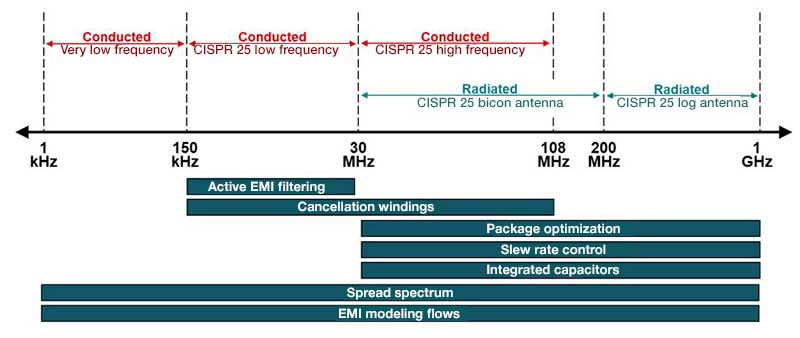
To resolve this trade-off and obtain the combined benefits of high power density, high efficiency and low EMI, a host of techniques as shown in Figure 5 are designed into TI’s switching converters and controllers, such as LM25149-Q1, LM5156-Q1 and LM62440-Q1. These techniques such as spread spectrum, active EMI filtering, cancellation windings, package innovations, integrated input bypass capacitors, and true slew-rate control methodologies are tailored to specific frequency bands of interest and are described in depth in the white paper linked above and related instructional videos linked in the additional resources section.
 Figure 5 Techniques Designed into TI’s
Power Converters and Controllers to Minimize EMI
Figure 5 Techniques Designed into TI’s
Power Converters and Controllers to Minimize EMIConclusion
Designing for low EMI can save you significant development cycle time while also reducing board area and solution cost. TI offers multiple features and technologies to mitigate EMI. Employing a combination of techniques with TI’s EMI-optimized power-management devices ensures that designs using TI components will pass industry standards without much rework. I hope this information and related content will simplify your design process and enable your end-equipment to remain under EMI limits without sacrificing power density or efficiency.
Additional Resources
- See ti.com/lowemi to learn more about TI products that use these mitigation technologies, including buck-boost and inverting regulators, isolated bias supplies, multichannel integrated circuits (PMIC), step-down (buck) regulators and step-up (boost) regulators.
- Explore this comprehensive training video series to learn more about the fundamentals of EMI, the various technologies that can help reduce emissions and more.
- For a comprehensive list of EMI standards, see the white papers, “An overview of conducted EMI specifications for power supplies” and “An overview of radiated EMI specifications for power supplies.”