SSZT109 December 2021 UCC27614 , UCC27624
The world is a noisy place – and power supplies are no exception. In the pursuit of higher efficiency, power converters switching at faster and faster speeds create unintended issues, including increasing the system’s susceptibility to transients and noise. It’s important to consider this susceptibility when choosing how to design your power supplies, and what components to design them with.
Where does the noise come from?
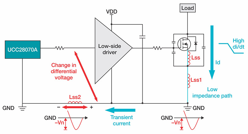
Where are the transients and noise coming from? Apart from the general noise found in many electrical systems, the high-frequency power supply itself often ends up generating them. Take a look at Figure 1, which shows a controller and a gate driver driving a metal-oxide semiconductor field-effect transistor (MOSFET).
 Figure 1 Transient current (di/dt) effect on the inputs of a gate driver in a power converter
As the gate driver switches the FET on and off, transients and noise are likely to occur. Parasitic trace inductances and the MOSFET’s source inductance, when combined with the fast switching of today’s power supplies, can lead to a situation known as ground bounce at the gate-driver’s integrated circuit (IC). Ground bounce is when the parasitic inductance of a system causes the ground of the IC to shift away from the ground of the system. The IC will register a 0-V signal as a negative voltage, which can cause damage or false logic outputs.
Not only is ground bounce a possible issue for the inputs, but the high switching speeds of many modern power supplies can also introduce negative voltage transients. Looking again at Figure 1, a large di/dt during switching that is proportional to the parasitic inductance (LSS) generates a negative voltage spike (Vn) . These negative transients are proportional to both parasitic inductances and frequency, so they grow more troublesome as the switching frequency increases.
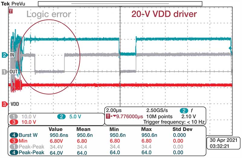
Voltage transients at the driver’s output also cause issues. Power supply output load changes are the most common cause of voltage transients. If these transients exceed the maximum voltage of the gate driver, they could end up damaging the device. Noise resulting from transients could even result in an output error, causing the driver to change its output regardless of the control signal, as shown in Figure 2.
 Figure 2 Driver response to noise on the outputs
The existing solution
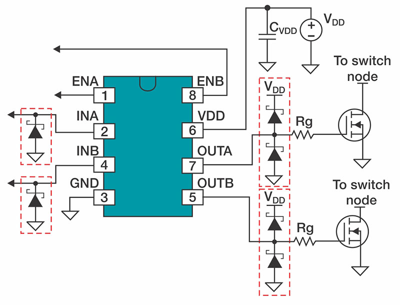
What can you do to address these transients, along with other noise? First of all taking the time to ensure proper board layout is important. Placing the driver as close to the switch as possible will help reduce the parasitic inductances. Doing so will not make the problem go away, however; it will just make it more manageable. In the past, a common solution to transients that could cause damage on the driver’s inputs or outputs was to add clamp diodes to hold the voltage above or below certain levels. Figure 3 shows an example of how to place these diodes.
 Figure 3 Clamp diodes on a gate driver’s inputs and outputs
The diodes on the input hold the input signal above ground, while the diodes on the output hold the voltage below the supply voltage (VDD). While effective, this is a costly solution, adding as many as six extra components to the power supply. Not only do these diodes add to the overall price of the system, they take up valuable space on the board.
Using 30-V gate drivers in your power-supply design
Newer gate drivers such as TI’s UCC27614 and UCC27624 can handle the noise and transients resulting from today’s higher-frequency power converters. These drivers offer –10-V negative voltage handling, which means that they can withstand the negative voltage shift brought on by ground bounce or negative voltage spikes caused by input transients without the need for external components. Not only do these drivers have the ability to handle lower voltages than many low-side drivers, they also have a 30-V maximum VDD. This is an important specification, because if the gate driver has enough headroom, it can handle noise and transients on its outputs without requiring clamp diodes to hold the output voltage below VDD.
Figure 4 shows the difference in how the 30-V UCC27624 and a 20-V VDD gate driver react to high-frequency noise on the outputs.
 Figure 4 Driver response to noise on the outputs
In this case, the 20-V VDD driver experiences a logic error from the noise, whereas the higher VDD of the UCC27624 eliminates errors without adding external components.
Conclusion
As electronics move forward, power supplies are going to keep moving to higher and higher frequencies in the quest to be more efficient, and transients will continue to grow with the frequency. When designing a power supply, remember that instead of adding extra components to your system to compensate, start with a driver that has the voltage range, negative voltage handling and reverse-current capability to address transients in your system.
Additional resources
- Read the application report, “Fundamentals of MOSFET and IGBT Gate Driver Circuits.”
- Check out the application note, “External Gate Resistor Design Guide for Gate Drivers.”