SNVU758 February 2021 TPSM13604H
3 Performance Data
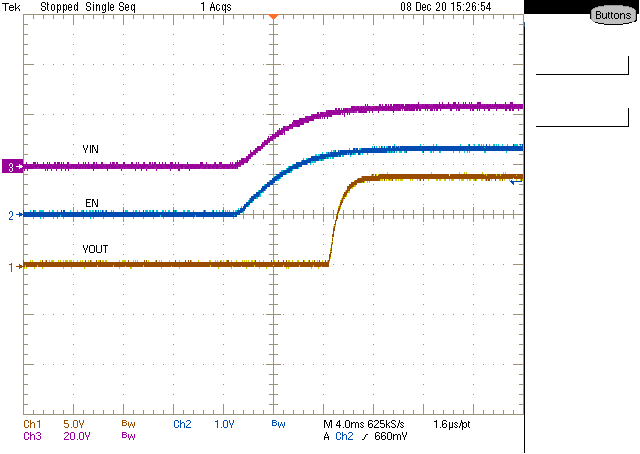
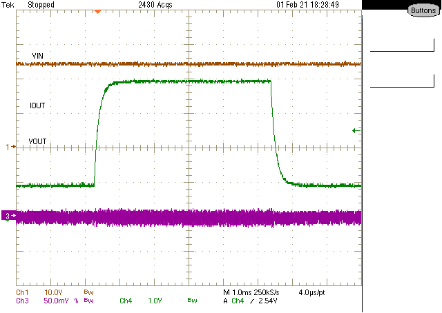
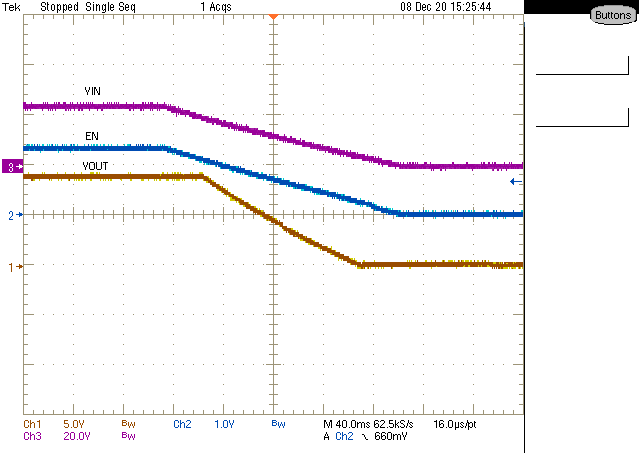
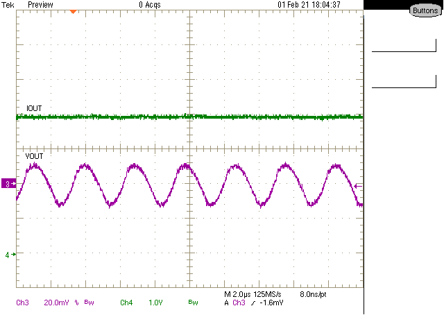
Figure 3-1 and Figure 3-2 shows the enable and shutdown of the TPSM13604HEVM. See Figure 3-3 for transient response waveforms (1-A to 4-A load step) and Figure 3-4 for output ripple. The default output capacitance configured on the EVM is optimized for an output voltage of 5.0-V and 3.3-V. The output voltage tested below are for an output voltage of 9-V and switching frequency of approximately 300-kHz by placing shunt on J4 Pins 5 and 6, changing R9 resistor to 3.32kΩ and R3 resistor to 232kΩ, and placing shunt on J3 Pins 5 and 6.
 Figure 3-1 TPSM13604HEVM ENABLE Start-Up Waveform
 Figure 3-3 TPSM13604HEVM Transient Performance (VIN = 24-V;
VOUT = 9-V; IOUT = 1-A to 4-A)
 Figure 3-2 TPSM13604HEVM ENABLE Shutdown Waveform
 Figure 3-4 TPSM13604HEVM Output Ripple (VIN = 24-V; VOUT =
9-V; IOUT = 4-A)