SNVU737A December 2020 – December 2021 LM5123-Q1
2.3.1 Output Voltage Tracking
Section 2.3.1describes how to setup the evaluation module for dynamic output voltage tracking.
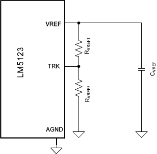
The LM5123EVM-BST is typically configured to have fixed output voltage of 24 V. Figure 2-2 shows the resistor divider connection from the REF pin to the TRK pin that sets the output voltage to 24 V. RVREFT is R24 and RVREFB is R26 referring to the schematic.
 Figure 2-2 Fixed Output Voltage Configuration
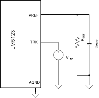
To dynamically change the output voltage, RVREFT and RVEFB are removed and the TRK pin voltage is driven directly to change the output voltage. See the data sheet for selecting the voltage range of the LM5123-Q1 and setting the TRK pin voltage to produce the desired output voltage. Figure 2-3 shows the configuration to change the output voltage dynamically. RSET is R25 in the schematic.
 Figure 2-3 Variable Output Voltage Configuration
 To recreate the waveforms in Section 4.7, RSET is set to be 24.9 kΩ and the TRK pin is driven between 400 mV and 550 mV, setting the output voltage to 24 V and 33V respectively.