SNVU585B February 2020 – November 2021 LMR43620-Q1
1.2 Jumpers
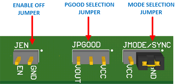
See Figure 1-2 for jumper locations.
- JEN — This jumper allows the ENABLE input to be connected to GND in order to disable the IC. By default, this jumper is left open since there is a pullup resistor, R2 (RENT), to VIN to enable the IC.
- JPGOOD — Use this jumper to select how the PGOOD pin is connected. A jumper can be used to connect pin 2 and 3. In this configuration, the PGOOD pin will be pulled up to VOUT through R7 (RPGOOD) with a value of 100 kΩ. When connecting the jumper between pin 1 and 2, the PGOOD pin will be pulled up to VCC through R7 (RPGOOD) with a value of 100 kΩ. By default, this jumper is not populated.
- JMODE/SYNC — Use this jumper to select the mode of operation in a
MODE/SYNC trim part.
Connecting a jumper between pin 1 and 2 sets the IC operation to PFM (pulse frequency modulation) mode for a higher efficiency at light load. A jumper between pin 2 and pin 3 causes the IC to operate in FPWM (forced pulse width modulation) mode. By default, the jumper is connected between pin 1 and 2. Pin 1 is indicated by the dot on the PCB.
 Figure 1-2 Jumper
Locations