SNVAA19 May 2021 LP8863-Q1 , LP8864-Q1 , LP8864S-Q1 , LP8866-Q1 , LP8866S-Q1
2 Boost Output Voltage Range Design Consideration
Feedback resistors are selected to ensure that the minimum boost voltage with ISEL = 0 μA is below the minimum LED string voltage, as shown in Equation 4. The maximum boost voltage with ISEL = 38.7 μA need to be at least 2 V greater than the maximum LED string voltage + the maximum headroom at LED sink pins as shown in Equation 2.
Equation 1. 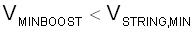
Equation 2. 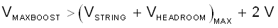
Where:
- VMINBOOST is the minimum boost voltage when ISEL = 0 μA (minimum)
- VMAXBOOST is the maximum boost voltage when ISEL = 38.7 μA (maximum)
- VSTRING is the voltage across LED string
- VHEADROOM is the headroom voltage of LED current sink and can be substituted with 1 V in Equation 2
- 2 V in Equation 2 is an empirical design margin considering the variations of internal reference and the tolerance of feedback resistors.