SNOU186 September 2021
- Trademarks
- 1Introduction
-
2Description
- 2.1 Input Power and Load (J1/J5 and J2/J6, J8/J12 and J9/J13):
- 2.2 Enable Control (J4 and J11):
- 2.3 Two Back-to-Back Connected MOSFETs (Q1/Q3-Q2/Q4 and M1/M3-M2/M4):
- 2.4 Output Slew Rate Control (R3 and C4, R10 and C13):
- 2.5 Output Schottky Diode (D3, D8) and LED Indication (D4, D10) :
- 2.6 TVS Selection for 12-V Battery Protection:
- 2.7 TVS Selection for 24-V Battery Protection:
- 2.8 Test Points:
- 3Schematic
- 4Test Equipment Requirements
- 5Test Setup and Results
- 6Board Layout and Bill of Materials
5 Test Setup and Results
This setup and results section describes the test procedure for LM74720-Q1 device. Similar procedure applies for LM74722-Q1 device also.
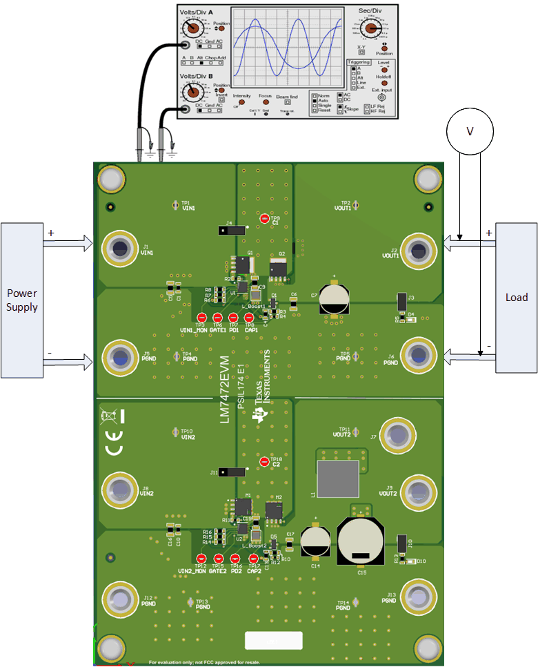
Default jumper setting for LM7472EVM board is shown in Figure 5-1.
Table 5-1 Default Jumper Setting for LM7472EVM
| J4 | J3 | J11 | J10 |
|---|---|---|---|
| 1-2 or connect 2 to external enable control | 1-2, Output LED Indication | 1-2 or connect 2 to external enable control | 1-2, Output LED Indication |
 Figure 5-1 LM7472EVM Test Setup