SNAU278 July 2022
9.2 Output Format Selection
The OE pin is used to enable or disable the output.
The OS pin is used to bias internal drivers and change the output format.
Table 9-2 Reference PRO Output Format Selection
| OE | OS | OUTPUT FORMAT |
|---|---|---|
| GND | Don't Care | Disabled |
| Vdd | GND | LVPECL |
| Vdd | NC | LVDS |
| Vdd | Vdd | HCSL |
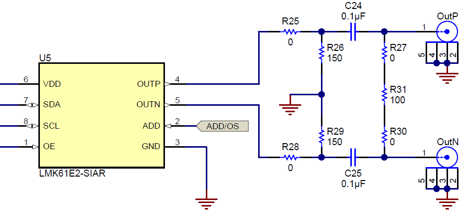
It is imperative to match the output termination passive components as shown in Table 9-3.
Table 9-3 Output Termination
Configuration
| OUTPUT FORMAT | COUPLING | COMPONENT | VALUE |
|---|---|---|---|
| LVPECL | AC (Default configuration) | R15, R28 | 0 Ω |
| R26, R29 | 150 Ω | ||
| C24, C25 | 0.01 µF | ||
| R27, R30, R31 | DNP | ||
| DC(1) | R15, R28, C24, C25 | 0 Ω | |
| R26, R27, R29, R30, R31 | DNP | ||
| LVDS(2) | AC | R25, R27, R28, R30 | 0 Ω |
| R31 | 100 Ω | ||
| C24, C25 | 0.01 µF | ||
| R26, R29 | DNP | ||
| DC | R25, R27, R28, R30, C24, C25 | 0 Ω | |
| R31 | 100 Ω | ||
| R26, R29 | DNP | ||
| HCSL | AC | R15, R28 | 0 Ω |
| R26, R29 | 50 Ω | ||
| C24, C25 | 0.01 µF | ||
| R27, R30, R31 | DNP | ||
| DC | R25, R28, C24, C25 | 0 Ω | |
| R26, R29 | 50 Ω | ||
| R27, R30, R31 | DNP |
(1) 50-Ω to VCC – 2-V termination is required on receiver.
(2) 100-Ω differential termination (R31) is provided onboard. Removing
this termination is possible if the differential termination is available on the
receiver.
 Figure 9-2 Output Termination
Schematic