SNAU278 July   2022


  1.   Abstract
  2.   Trademarks
  3. 1LMX2594PSEVM Evaluation Module
    1. 1.1 Evaluation Module Contents
    2. 1.2 Evaluation Setup Requirement
    3. 1.3 Resources
  4. 2Setup
    1. 2.1 Connection Diagram
    2. 2.2 Power Supply
    3. 2.3 Reference Clock
    4. 2.4 SYNC Input
    5. 2.5 RF Output
    6. 2.6 Programming
    7. 2.7 Evaluation Software
  5. 3Typical Measurement
    1. 3.1 Category 3 Synchronization
    2. 3.2 Phase Noise Improvement
  6. 4Schematic
  7. 5PCB Layout and Layer Stack-up
    1. 5.1 PCB Layer Stack-Up
    2. 5.2 PCB Layout
  8. 6Bill of Materials
  9. 7EVM Modification
  10. 8Troubleshooting Guide
  11. 9Reference PRO
    1. 9.1 Output Frequency Selection
    2. 9.2 Output Format Selection
    3. 9.3 Typical Output Characteristics
    4. 9.4 Firmware Update

EVM Modification

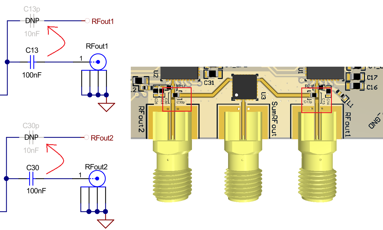
The default EVM configuration has the outputs of the LMX2594 devices connected to the RFout1 and RFout2 SMA connectors. To evaluate the phase noise improvement by summing the two outputs together, do the following modifications.

  • Move C13 to C13p
  • Move C30 to C30p

GUID-20220721-SS0I-XT6G-HM3R-4VDBS23NQQF1-low.pngFigure 7-1 EVM Modification for Phase Noise Reduction