SNAS407H August 2007 – April 2015 DAC128S085
PRODUCTION DATA.
- 1 Features
- 2 Applications
- 3 Description
- 4 Revision History
- 5 Description (continued)
- 6 Pin Configuration and Functions
- 7 Specifications
- 8 Detailed Description
- 9 Application and Implementation
- 10Power Supply Recommendations
- 11Layout
- 12Device and Documentation Support
- 13Mechanical, Packaging, and Orderable Information
7 Specifications
7.1 Absolute Maximum Ratings
over operating free-air temperature range (unless otherwise noted)(1)(1)| MIN | MAX | UNIT | ||
|---|---|---|---|---|
| Supply Voltage, VA | 6.5 | V | ||
| Voltage on any Input Pin | −0.3 | 6.5 | V | |
| Input Current at Any Pin(2) | 10 | mA | ||
| Package Input Current(2) | 30 | mA | ||
| Power Consumption at TA = 25°C | See (3) | |||
| Junction Temperature | 150 | °C | ||
| Storage Temperature, Tstg | −65 | 150 | °C | |
(1) All voltages are measured with respect to GND = 0 V, unless otherwise specified.
(2) When the input voltage at any pin exceeds 5.5 V or is less than GND, the current at that pin should be limited to 10 mA. The 30-mA maximum package input current rating limits the number of pins that can safely exceed the power supplies with an input current of 10 mA to three.
(3) The absolute maximum junction temperature (TJmax) for this device is 150°C. The maximum allowable power dissipation is dictated by TJmax, the junction-to-ambient thermal resistance (RθJA), and the ambient temperature (TA), and can be calculated using the formula PDMAX = (TJmax − TA) / RθJA. The values for maximum power dissipation will be reached only when the device is operated in a severe fault condition (for example, when input or output pins are driven beyond the operating ratings, or the power supply polarity is reversed). Such conditions should always be avoided.
7.2 ESD Ratings
| VALUE | UNIT | |||
|---|---|---|---|---|
| V(ESD) | Electrostatic discharge | Human body model (HBM), per ANSI/ESDA/JEDEC JS-001(1) | ±2500 | V |
| Charged-device model (CDM), per JEDEC specification JESD22-C101(2) | ±1000 | |||
| Machine Model | ±250 | |||
(1) JEDEC document JEP155 states that 500-V HBM allows safe manufacturing with a standard ESD control process.
(2) JEDEC document JEP157 states that 250-V CDM allows safe manufacturing with a standard ESD control process.
7.3 Recommended Operating Conditions
over operating free-air temperature range (unless otherwise noted)| MIN | MAX | UNIT | ||
|---|---|---|---|---|
| Operating Temperature Range | −40 ≤ TA ≤ +125 | °C | ||
| Supply Voltage, VA | 2.7 | 5.5 | V | |
| Reference Voltage, VREF1,2 | 0.5 | VA | V | |
| Digital Input Voltage(1) | 0.0 | 5.5 | V | |
| Output Load | 0 | 1500 | pF | |
| SCLK Frequency | 40 | MHz | ||
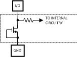
(1) The inputs are protected as shown below. Input voltage magnitudes up to 5.5 V, regardless of VA, will not cause errors in the conversion result. For example, if VA is 3 V, the digital input pins can be driven with a 5-V logic device.

7.4 Thermal Information
| THERMAL METRIC(1) | DAC128S085 | UNIT | ||
|---|---|---|---|---|
| PW (TSSOP) | RGH (WQFN) | |||
| 16 PINS | 16 PINS | |||
| RθJA | Junction-to-ambient thermal resistance | 98 | 34 | °C/W |
| RθJA | Junction-to-ambient thermal resistance | 31 | 25 | |
| RθJA | Junction-to-ambient thermal resistance | 43 | 11 | |
| φJT | Junction-to-top characterization parameter | 2 | 0.2 | |
| φJB | Junction-to-board characterization parameter | 43 | 11 | |
(1) For more information about traditional and new thermal metrics, see the IC Package Thermal Metrics application report, SPRA953.
7.5 Electrical Characteristics
The following specifications apply for VA = 2.7 V to 5.5 V, VREF1 = VREF2 = VA, CL = 200 pF to GND, fSCLK = 30 MHz, input code range 48 to 4047. All limits are at TA = 25°C, unless otherwise specified.| PARAMETER | TEST CONDITIONS | MIN(2) | TYP | MAX(2) | UNIT | ||
|---|---|---|---|---|---|---|---|
| STATIC PERFORMANCE | |||||||
| Resolution | TMIN ≤ TA ≤ TMAX | 12 | Bits | ||||
| Monotonicity | TMIN ≤ TA ≤ TMAX | 12 | Bits | ||||
| INL | Integral Non-Linearity | ±2 | LSB | ||||
| TMIN ≤ TA ≤ TMAX | ±8 | ||||||
| DNL | Differential Non-Linearity | 0.15 | LSB | ||||
| TMIN ≤ TA ≤ TMAX | 0.75 | ||||||
| −0.09 | LSB | ||||||
| TMIN ≤ TA ≤ TMAX | −0.4 | ||||||
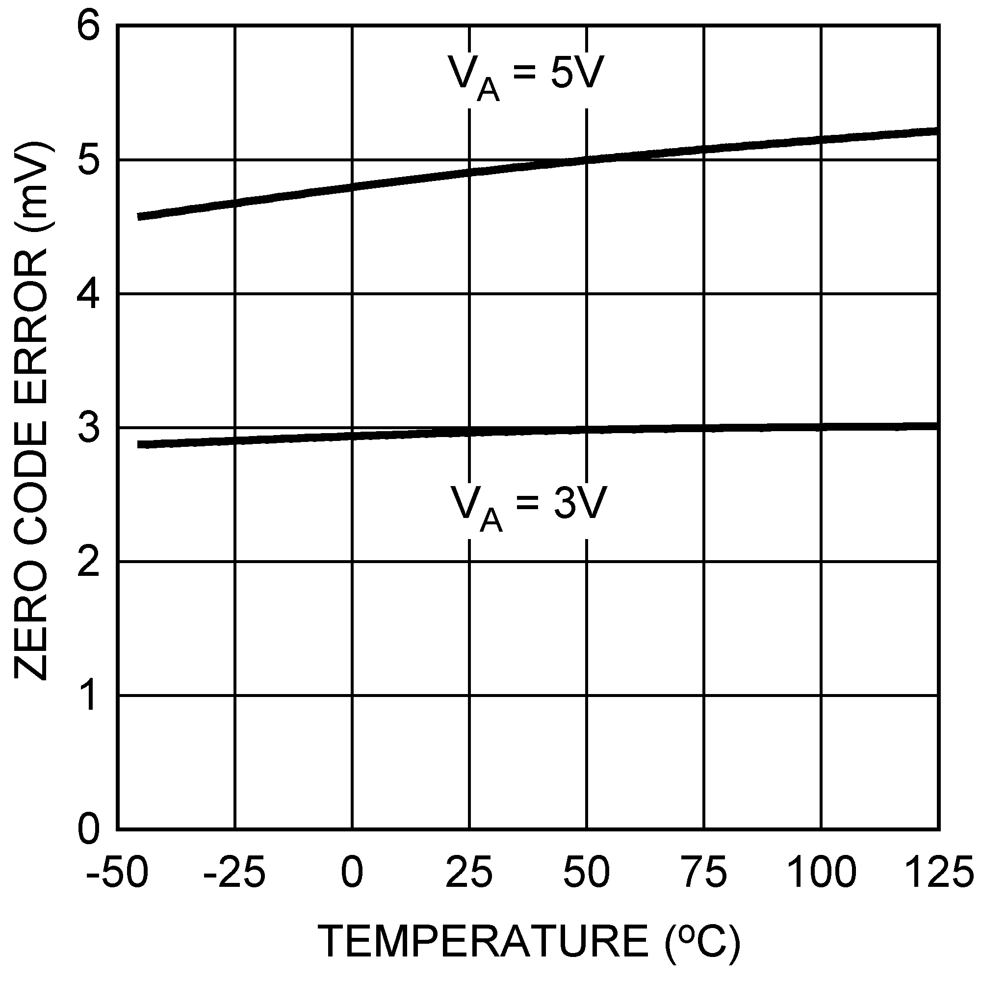
| ZE | Zero Code Error | IOUT = 0 | +5 | mV | |||
| TMIN ≤ TA ≤ TMAX | 15 | ||||||
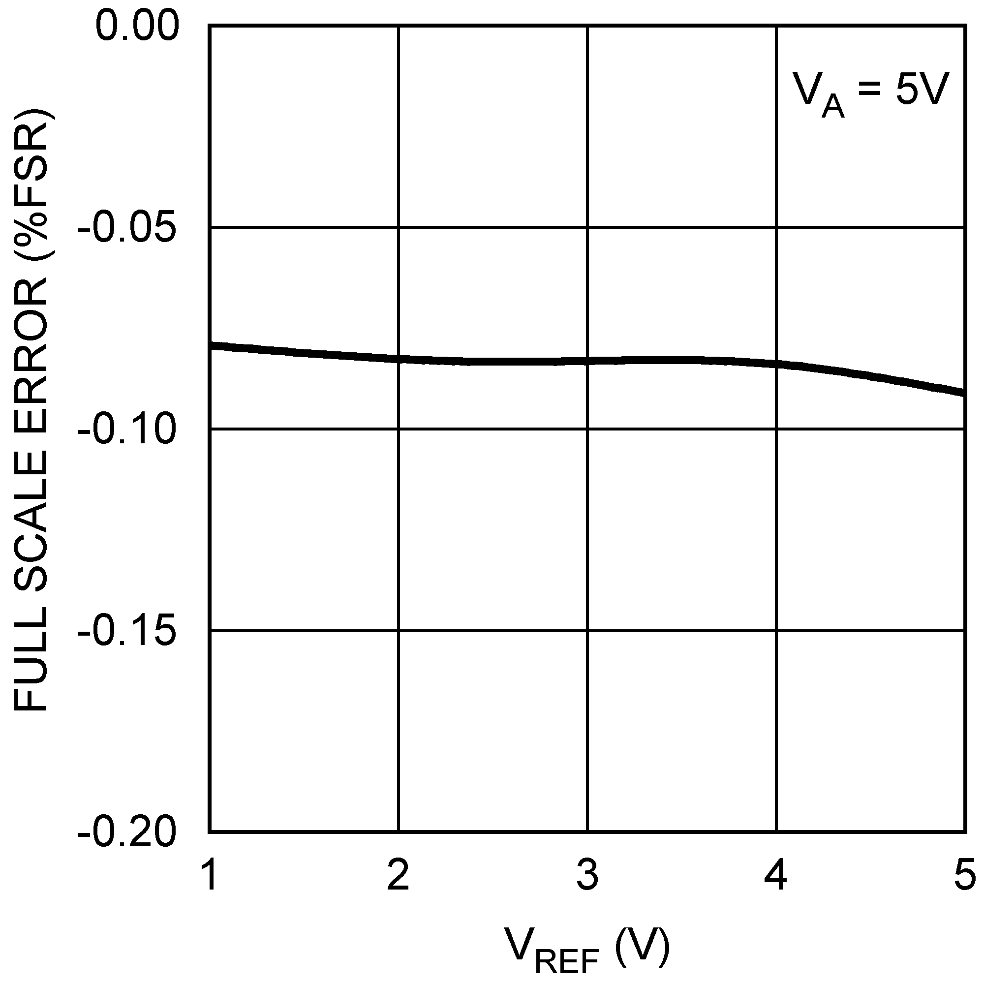
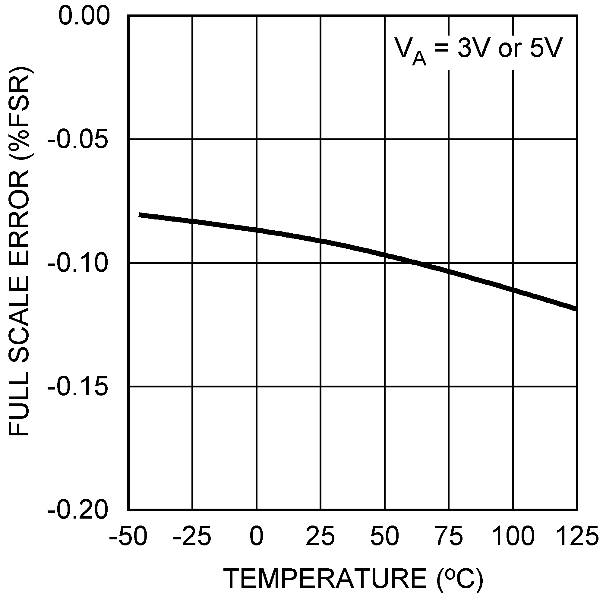
| FSE | Full-Scale Error | IOUT = 0 | −0.1% | FSR | |||
| TMIN ≤ TA ≤ TMAX | −0.75% | ||||||
| GE | Gain Error | −0.2% | FSR | ||||
| TMIN ≤ TA ≤ TMAX | −1 % | ||||||
| ZCED | Zero Code Error Drift | −20 | µV/°C | ||||
| TC GE | Gain Error Tempco | −1 | ppm/°C | ||||
| OUTPUT CHARACTERISTICS | |||||||
| Output Voltage Range | TMIN ≤ TA ≤ TMAX | 0 | VREF1,2 | V | |||
| IOZ | High-Impedance Output Leakage Current(3) |
TMIN ≤ TA ≤ TMAX | ±1 | µA | |||
| ZCO | Zero Code Output | VA = 3 V, IOUT = 200 µA | 10 | mV | |||
| VA = 3 V, IOUT = 1 mA | 45 | mV | |||||
| VA = 5 V, IOUT = 200 µA | 8 | mV | |||||
| VA = 5 V, IOUT = 1 mA | 34 | mV | |||||
| FSO | Full Scale Output | VA = 3 V, IOUT = 200 µA | 2.984 | V | |||
| VA = 3 V, IOUT = 1 mA | 2.933 | V | |||||
| VA = 5 V, IOUT = 200 µA | 4.987 | V | |||||
| VA = 5 V, IOUT = 1 mA | 4.955 | V | |||||
| IOS | Output Short Circuit Current (source)(4) | VA = 3 V, VOUT = 0 V, Input Code = FFFh |
−50 | mA | |||
| VA = 5 V, VOUT = 0 V, Input Code = FFFh |
−60 | mA | |||||
| IOS | Output Short Circuit Current (sink)(4) | VA = 3 V, VOUT = 3 V, Input Code = 000h |
50 | mA | |||
| VA = 5 V, VOUT = 5 V, Input Code = 000h |
70 | mA | |||||
| IO | Continuous Output Current per channel(3) | TA = 105°C TMIN ≤ TA ≤ TMAX |
10 | mA | |||
| TA = 125°C TMIN ≤ TA ≤ TMAX |
6.5 | mA | |||||
| CL | Maximum Load Capacitance | RL = ∞ | 1500 | pF | |||
| RL = 2 kΩ | 1500 | pF | |||||
| ZOUT | DC Output Impedance | 8 | Ω | ||||
| REFERENCE INPUT CHARACTERISTICS | |||||||
| VREF1,2 | Input Range Minimum | 0.5 | V | ||||
| TMIN ≤ TA ≤ TMAX | 2.7 | ||||||
| Input Range Maximum | TMIN ≤ TA ≤ TMAX | VA | V | ||||
| Input Impedance | 30 | kΩ | |||||
| LOGIC INPUT CHARACTERISTICS | |||||||
| IIN | Input Current(3) | TMIN ≤ TA ≤ TMAX | ±1 | µA | |||
| VIL | Input Low Voltage | VA = 2.7 V to 3.6 V | 1 | V | |||
| TMIN ≤ TA ≤ TMAX | 0.6 | ||||||
| VA = 4.5 V to 5.5 V | 1.1 | V | |||||
| 0.8 | |||||||
| VIH | Input High Voltage | VA = 2.7 V to 3.6 V | 1.4 | V | |||
| TMIN ≤ TA ≤ TMAX | 2.1 | ||||||
| VA = 4.5 V to 5.5 V | 2 | V | |||||
| TMIN ≤ TA ≤ TMAX | 2.4 | ||||||
| CIN | Input Capacitance(3) | TMIN ≤ TA ≤ TMAX | 3 | pF | |||
| POWER REQUIREMENTS | |||||||
| VA | Supply Voltage Minimum | TMIN ≤ TA ≤ TMAX | 2.7 | V | |||
| Supply Voltage Maximum | TMIN ≤ TA ≤ TMAX | 5.5 | V | ||||
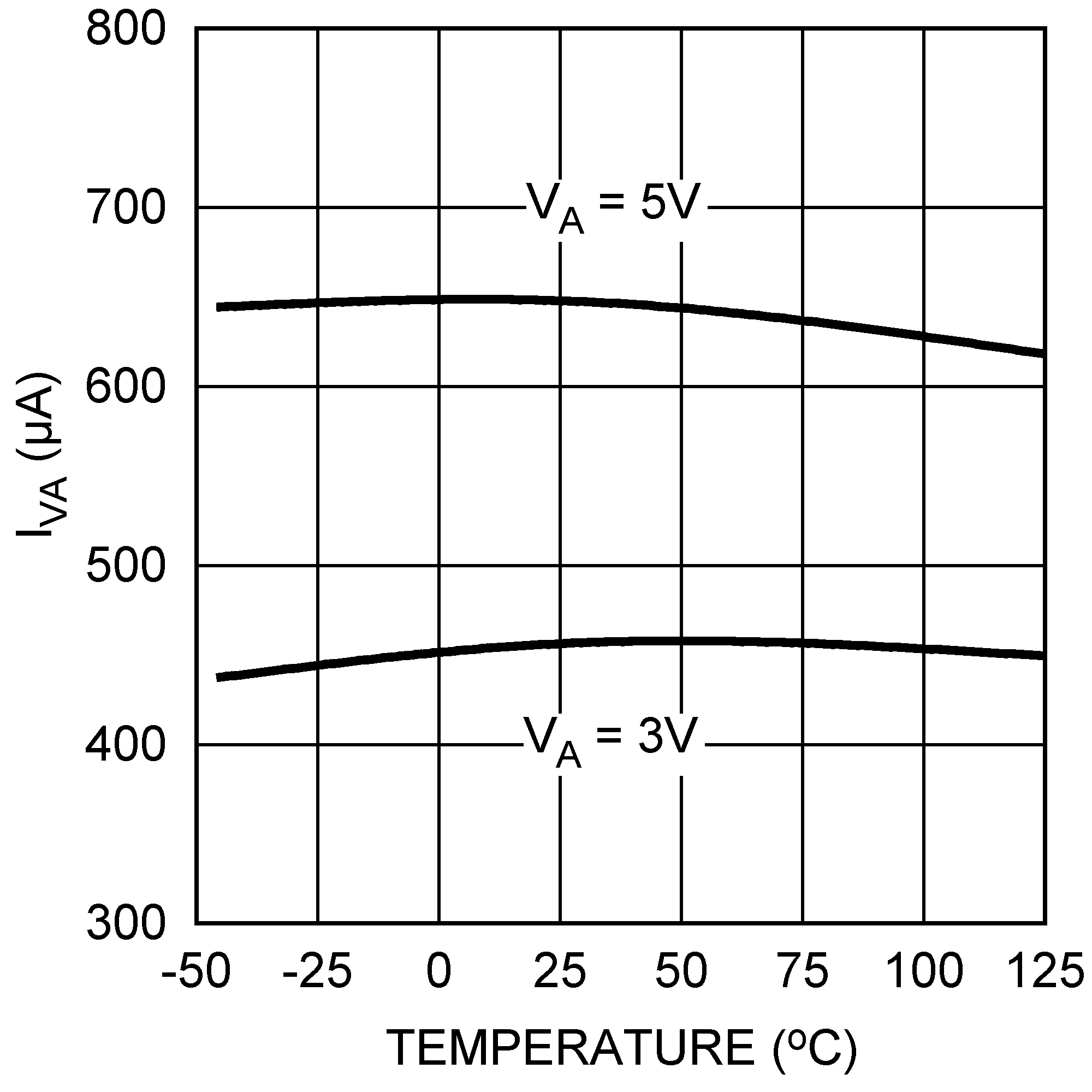
| IN | Normal Supply Current for supply pin VA | fSCLK = 30 MHz, output unloaded |
VA = 2.7 V to 3.6 V | 460 | µA | ||
| TMIN ≤ TA ≤ TMAX | 560 | ||||||
| VA = 4.5 V to 5.5 V | 650 | µA | |||||
| 830 | |||||||
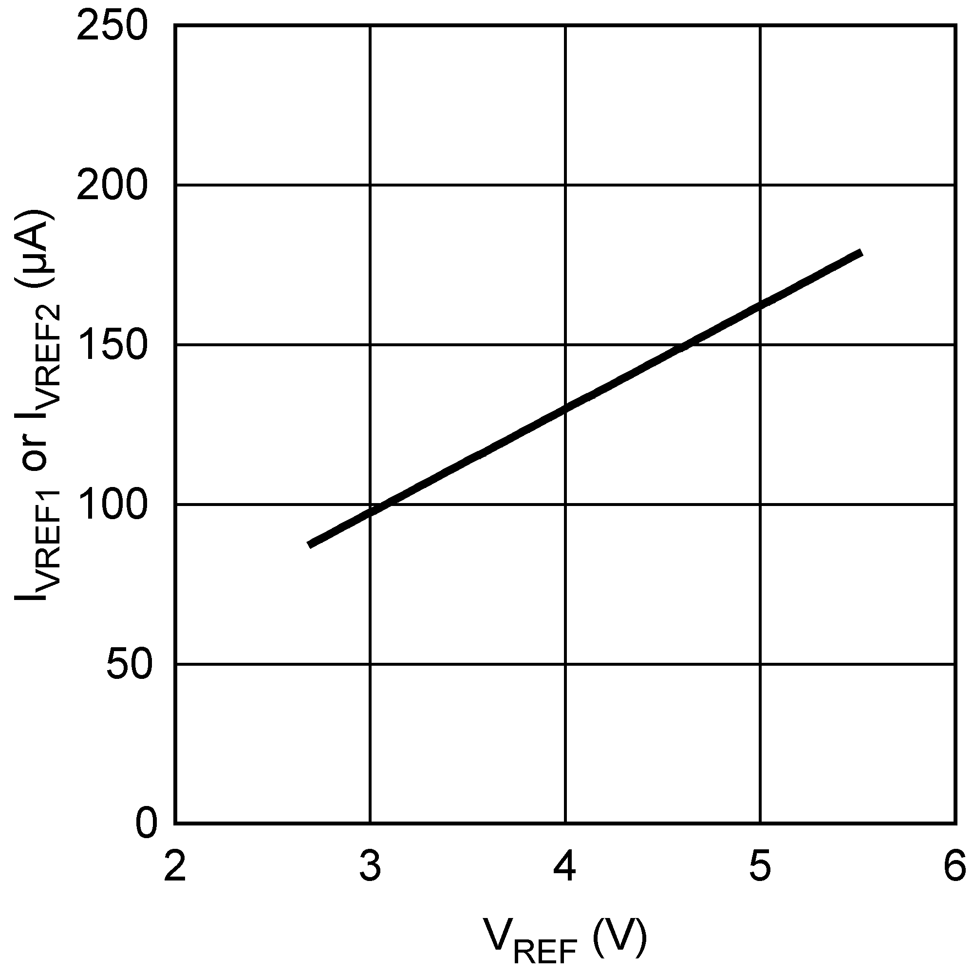
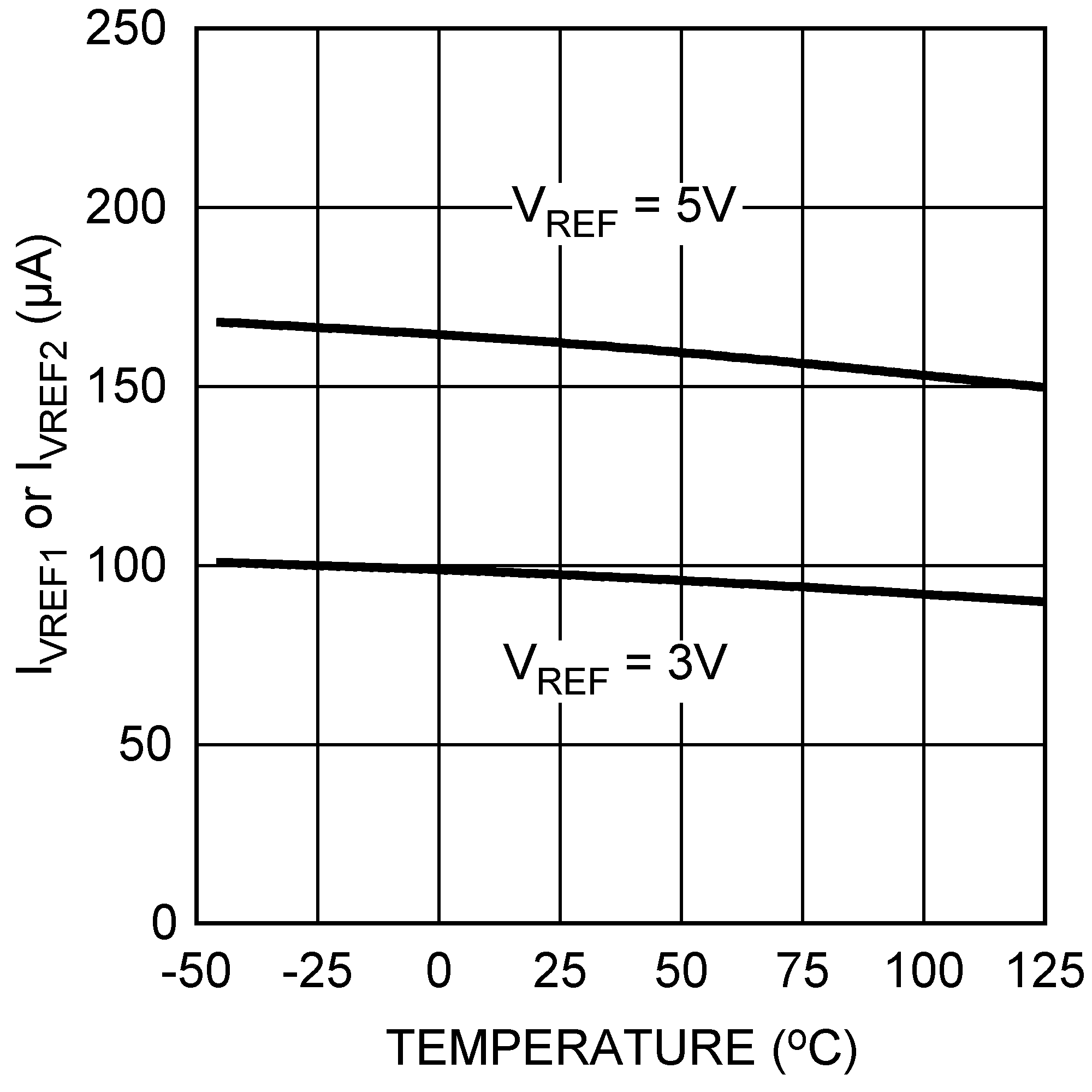
| Normal Supply Current for VREF1 or VREF2 | fSCLK = 30 MHz, output unloaded |
VA = 2.7 V to 3.6 V | 95 | µA | |||
| TMIN ≤ TA ≤ TMAX | 130 | ||||||
| VA = 4.5 V to 5.5 V | 160 | µA | |||||
| 220 | |||||||
| IST | Static Supply Current for supply pin VA | fSCLK = 0, output unloaded |
VA = 2.7 V to 3.6 V | 370 | µA | ||
| VA = 4.5 V to 5.5 V | 440 | µA | |||||
| Static Supply Current for VREF1 or VREF2 | fSCLK = 0, output unloaded |
VA = 2.7 V to 3.6 V | 95 | µA | |||
| VA = 4.5 V to 5.5 V | 160 | µA | |||||
| IPD | Total Power Down Supply Current for all PD Modes (3) |
fSCLK = 30 MHz, SYNC = VA and DIN = 0V after PD mode loaded | VA = 2.7 V to 3.6 V | 0.2 | µA | ||
| 1.5 | |||||||
| VA = 4.5 V to 5.5 V | 0.5 | µA | |||||
| TMIN ≤ TA ≤ TMAX | 3 | ||||||
| fSCLK = 0, SYNC = VA and DIN = 0V after PD mode loaded | VA = 2.7 V to 3.6 V | 0.1 | µA | ||||
| TMIN ≤ TA ≤ TMAX | 1 | ||||||
| VA = 4.5 V to 5.5 V | 0.2 | µA | |||||
| TMIN ≤ TA ≤ TMAX | 2 | ||||||
| PN | Total Power Consumption (output unloaded) | fSCLK = 30 MHz output unloaded |
VA = 2.7 V to 3.6 V | 1.95 | mW | ||
| TMIN ≤ TA ≤ TMAX | 3 | ||||||
| VA = 4.5 V to 5.5 V | 4.85 | mW | |||||
| TMIN ≤ TA ≤ TMAX | 7 | ||||||
| fSCLK = 0 output unloaded |
VA = 2.7 V to 3.6 V | 1.68 | mW | ||||
| VA = 4.5 V to 5.5 V | 3.80 | mW | |||||
| PPD | Total Power Consumption in all PD Modes, (3) |
fSCLK = 30 MHz, SYNC = VA and DIN = 0V after PD mode loaded | VA = 2.7 V to 3.6 V | 0.6 | µW | ||
| TMIN ≤ TA ≤ TMAX | 5.4 | ||||||
| VA = 4.5V to 5.5V | 2.5 | µW | |||||
| TMIN ≤ TA ≤ TMAX | 16.5 | ||||||
| fSCLK = 0, SYNC = VA and DIN = 0V after PD mode loaded | VA = 2.7 V to 3.6 V | 0.3 | µW | ||||
| TMIN ≤ TA ≤ TMAX | 3.6 | ||||||
| VA = 4.5 V to 5.5 V | 1 | µW | |||||
| TMIN ≤ TA ≤ TMAX | 11 | ||||||
7.6 AC and Timing Characteristics
The following specifications apply for VA = 2.7 V to 5.5 V, VREF1,2 = VA, CL = 200 pF to GND, fSCLK = 30 MHz, input code range 48 to 4047. All limits are at TA = 25°C, unless otherwise specified.| MIN(2) | NOM | MAX(2) | UNIT | ||||
|---|---|---|---|---|---|---|---|
| fSCLK | SCLK Frequency | 40 | MHz | ||||
| TMIN ≤ TA ≤ TMAX | 30 | ||||||
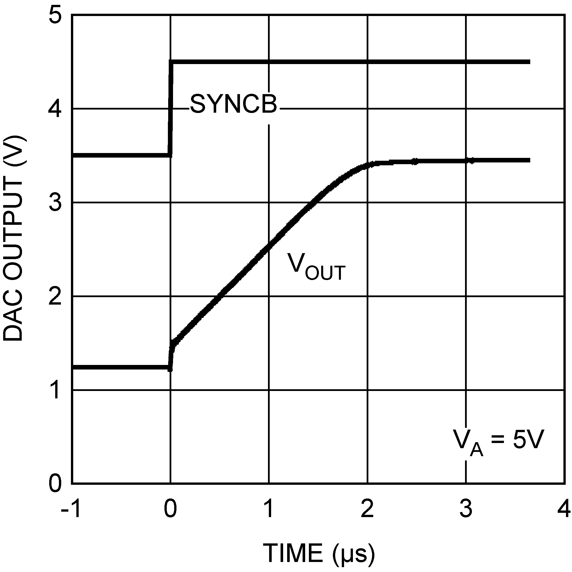
| ts | Output Voltage Settling Time (3) |
400h to C00h code change RL = 2 kΩ, CL = 200 pF |
6 | µs | |||
| TMIN ≤ TA ≤ TMAX | 8.5 | ||||||
| SR | Output Slew Rate | 1 | V/µs | ||||
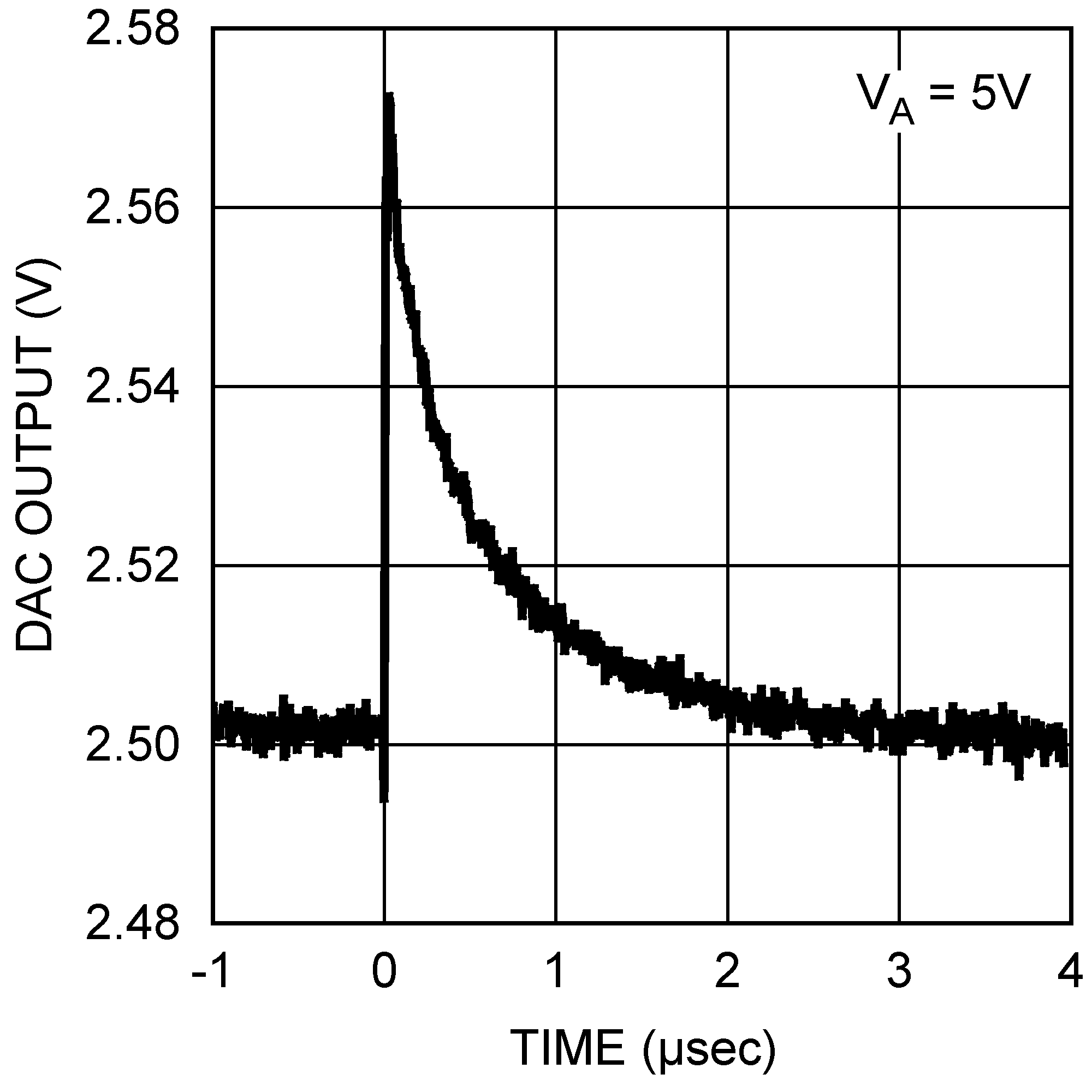
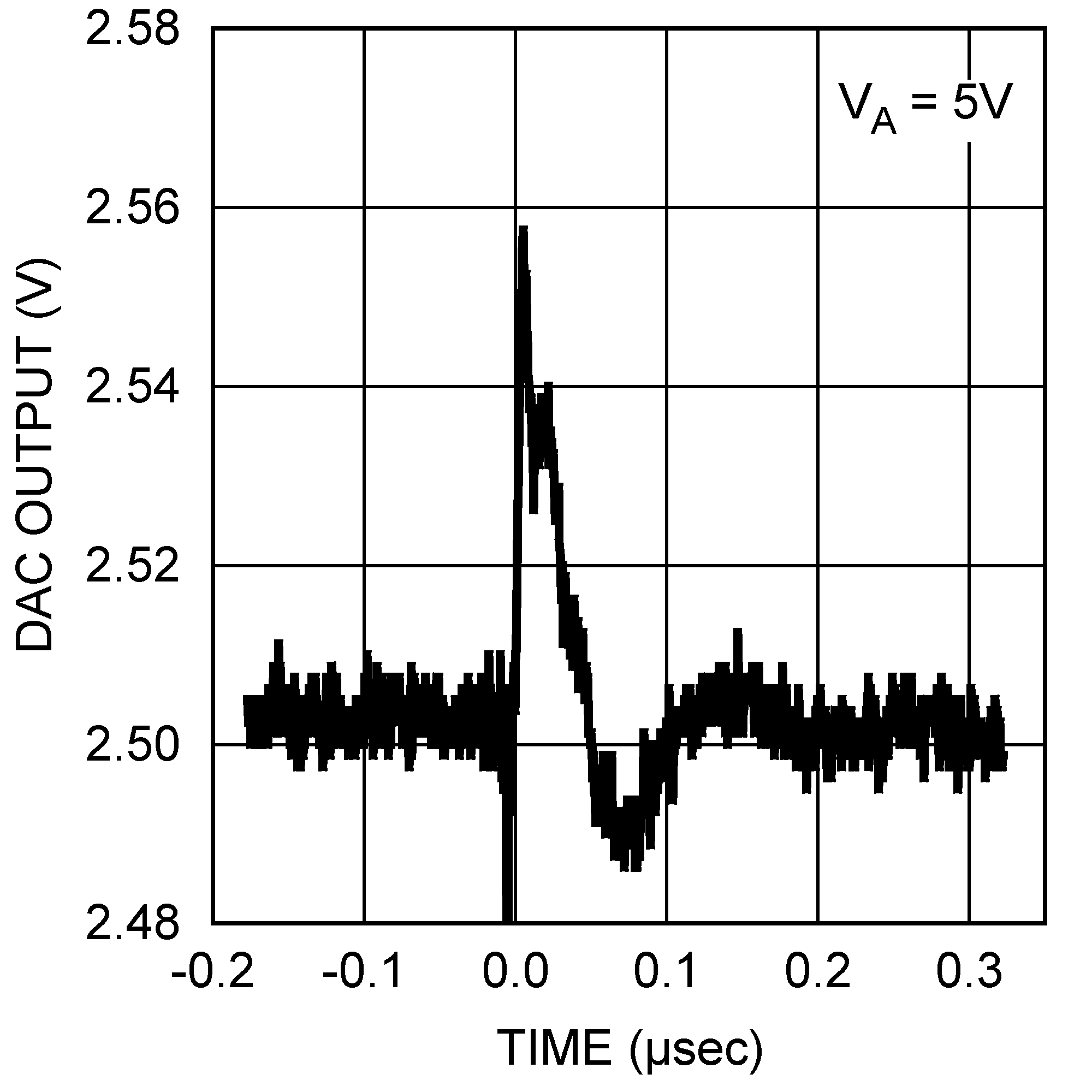
| GI | Glitch Impulse | Code change from 800h to 7FFh | 40 | nV-sec | |||
| DF | Digital Feedthrough | 0.5 | nV-sec | ||||
| DC | Digital Crosstalk | 0.5 | nV-sec | ||||
| CROSS | DAC-to-DAC Crosstalk | 1 | nV-sec | ||||
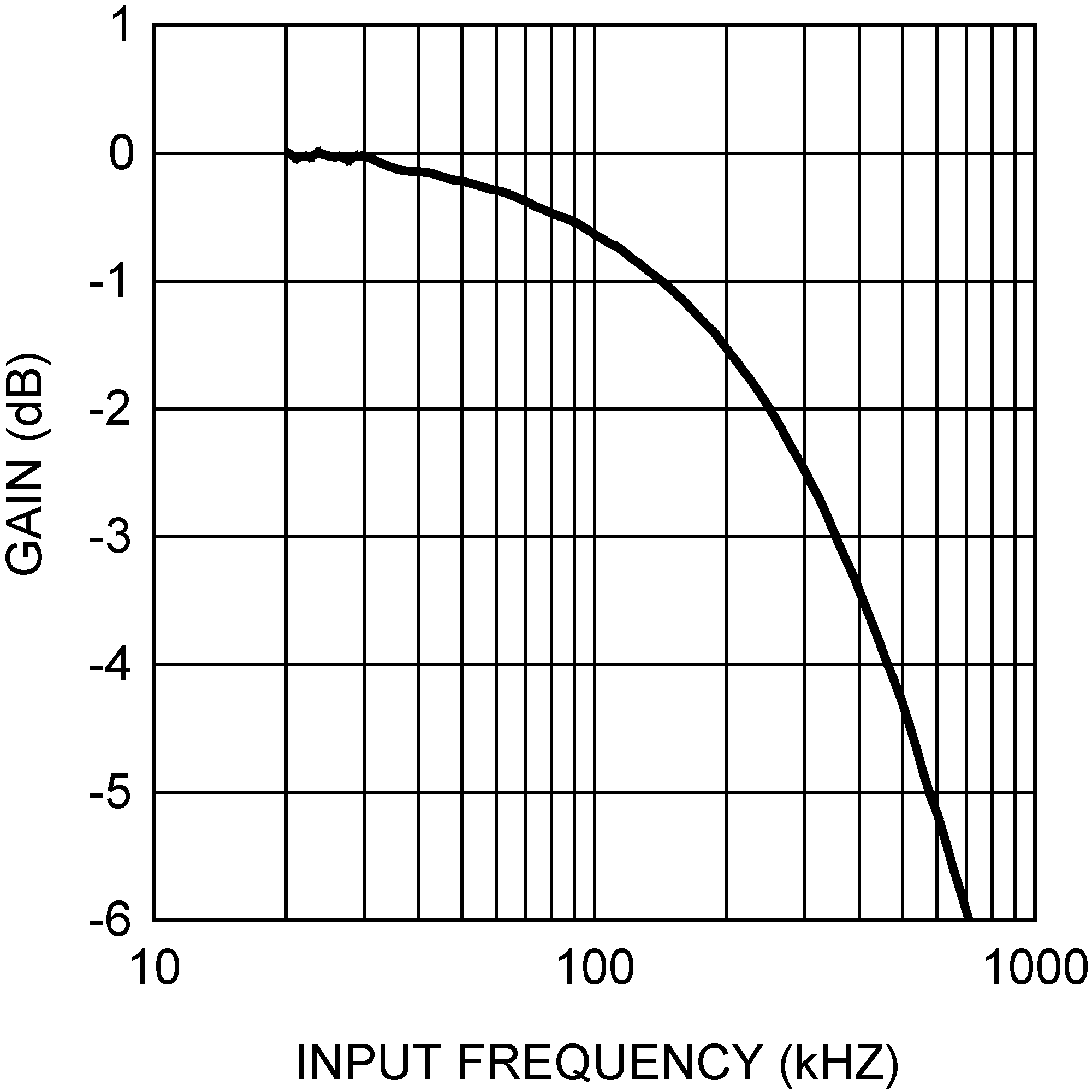
| MBW | Multiplying Bandwidth | VREF1,2 = 2.5 V ± 2 Vpp | 360 | kHz | |||
| THD+N | Total Harmonic Distortion Plus Noise | VREF1,2 = 2.5 V ± 0.5 Vpp 100 Hz < fIN < 20 kHz |
−80 | dB | |||
| ONSD | Output Noise Spectral Density | DAC Code = 800 h, 10 kHz | 40 | nV/sqrt (Hz) | |||
| ON | Output Noise | BW = 30 kHz | 14 | µV | |||
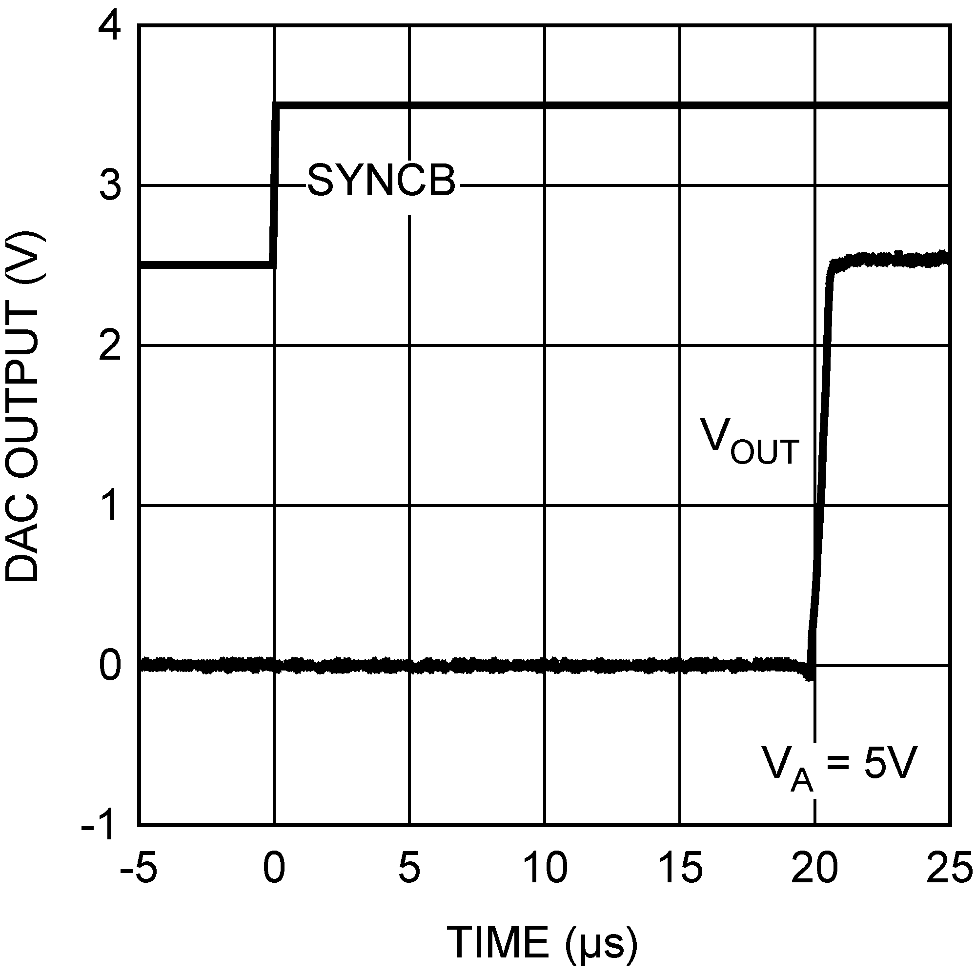
| tWU | Wake-Up Time | VA = 3 V | 3 | µsec | |||
| VA = 5 V | 20 | µsec | |||||
| 1/fSCLK | SCLK Cycle Time. See Figure 1 | 25 | ns | ||||
| TMIN ≤ TA ≤ TMAX | 33 | ||||||
| tCH | SCLK High time. See Figure 1 | 7 | ns | ||||
| TMIN ≤ TA ≤ TMAX | 10 | ||||||
| tCL | SCLK Low Time. See Figure 1 | 7 | ns | ||||
| TMIN ≤ TA ≤ TMAX | 10 | ||||||
| tSS | SYNC Set-up Time prior to SCLK Falling Edge. See Figure 1 | 3 | 1 / fSCLK - 3 | ns | |||
| TMIN ≤ TA ≤ TMAX | 10 | ||||||
| tDS | Data Set-Up Time prior to SCLK Falling Edge. See Figure 1 | 1 | ns | ||||
| TMIN ≤ TA ≤ TMAX | 2.5 | ||||||
| tDH | Data Hold Time after SCLK Falling Edge. See Figure 1 | 1 | ns | ||||
| TMIN ≤ TA ≤ TMAX | 2.5 | ||||||
| tSH | SYNC Hold Time after the 16th falling edge of SCLK. See Figure 1 | 0 | 1 / fSCLK - 3 | ns | |||
| TMIN ≤ TA ≤ TMAX | 3 | ||||||
| tSYNC | SYNC High Time. See Figure 1 | 5 | ns | ||||
| TMIN ≤ TA ≤ TMAX | 15 | ||||||
(1) Absolute Maximum Ratings indicate limits beyond which damage to the device may occur. Recomended Operating Ratings indicate conditions for which the device is functional, but do not specify specific performance limits. For ensured specifications and test conditions, see Electrical Characteristics. The ensured specifications apply only for the test conditions listed. Some performance characteristics may degrade when the device is not operated under the listed test conditions. Operation of the device beyond the Absolute Maximum Ratings is not recommended.
(2) Test limits are ensured to TI's AOQL (Average Outgoing Quality Level).
(3) This parameter is ensured by design and/or characterization and is not tested in production.
(4) This parameter does not represent a condition which the DAC can sustain continuously. See the continuous output current specification for the maximum DAC output current per channel.
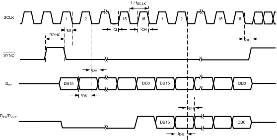 Figure 1. Serial Timing Diagram
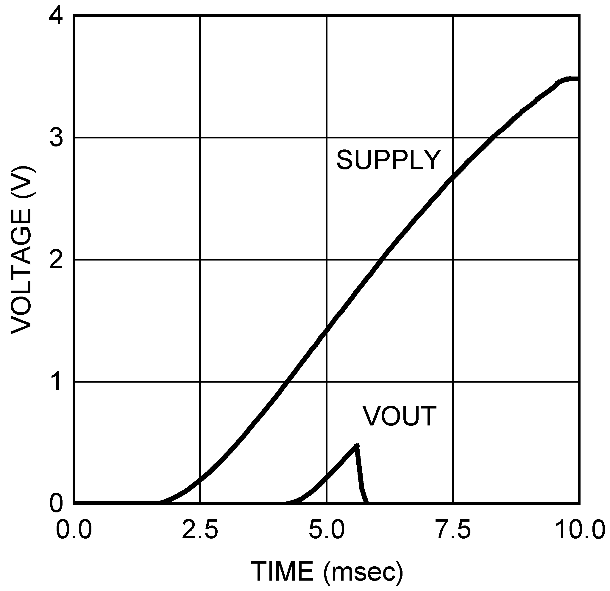
7.7 Typical Characteristics
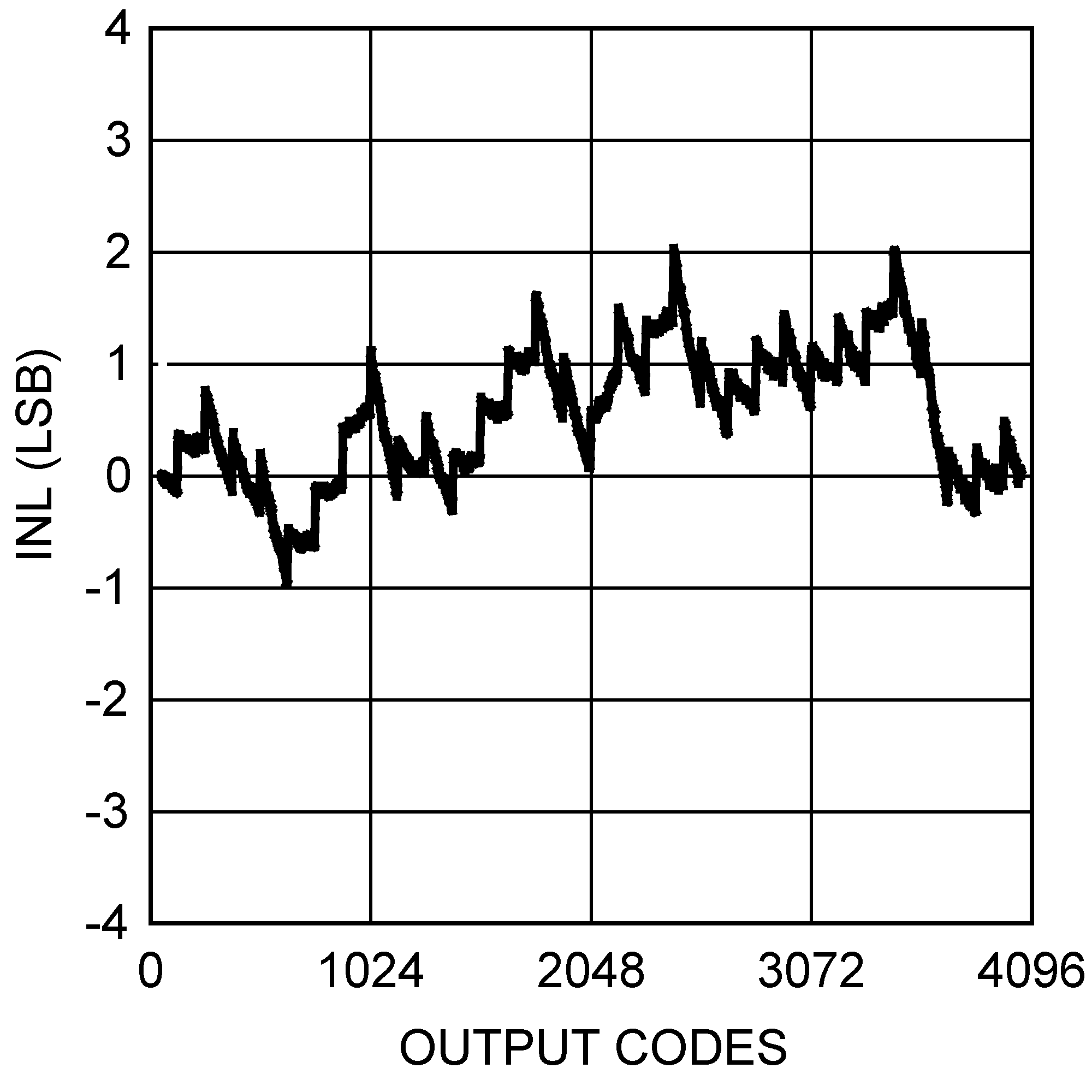
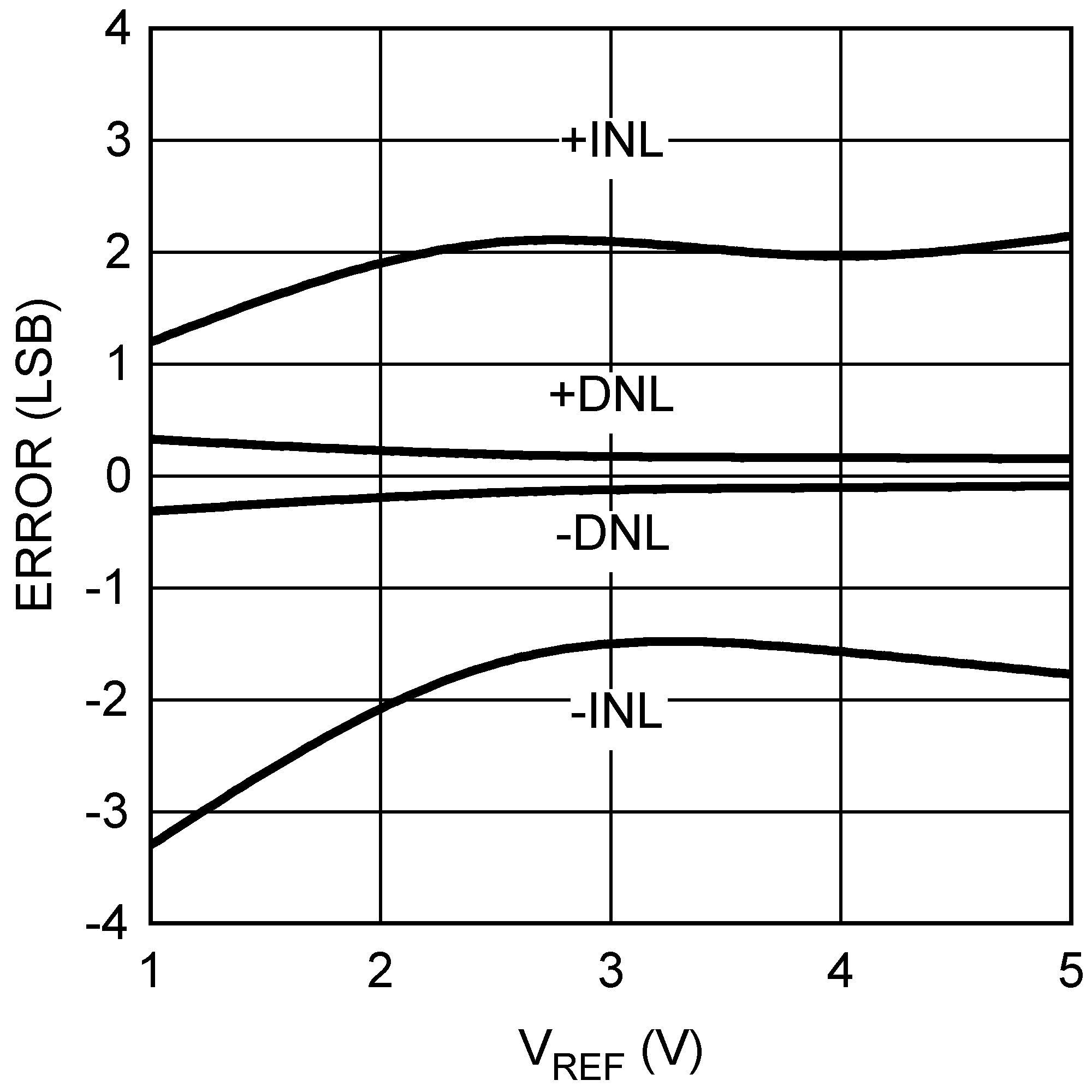
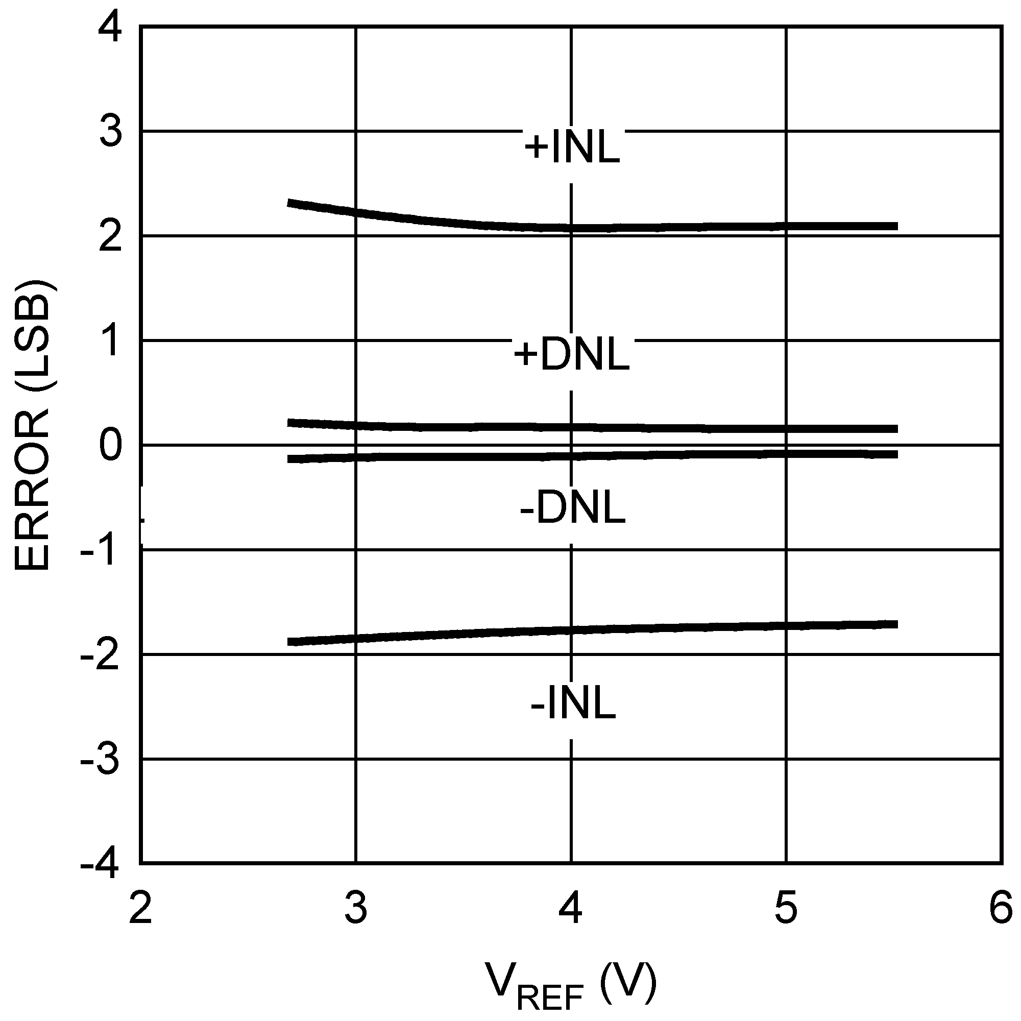
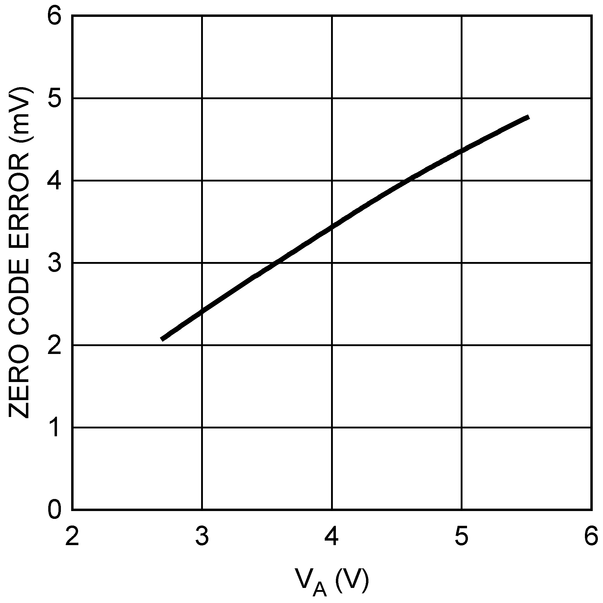
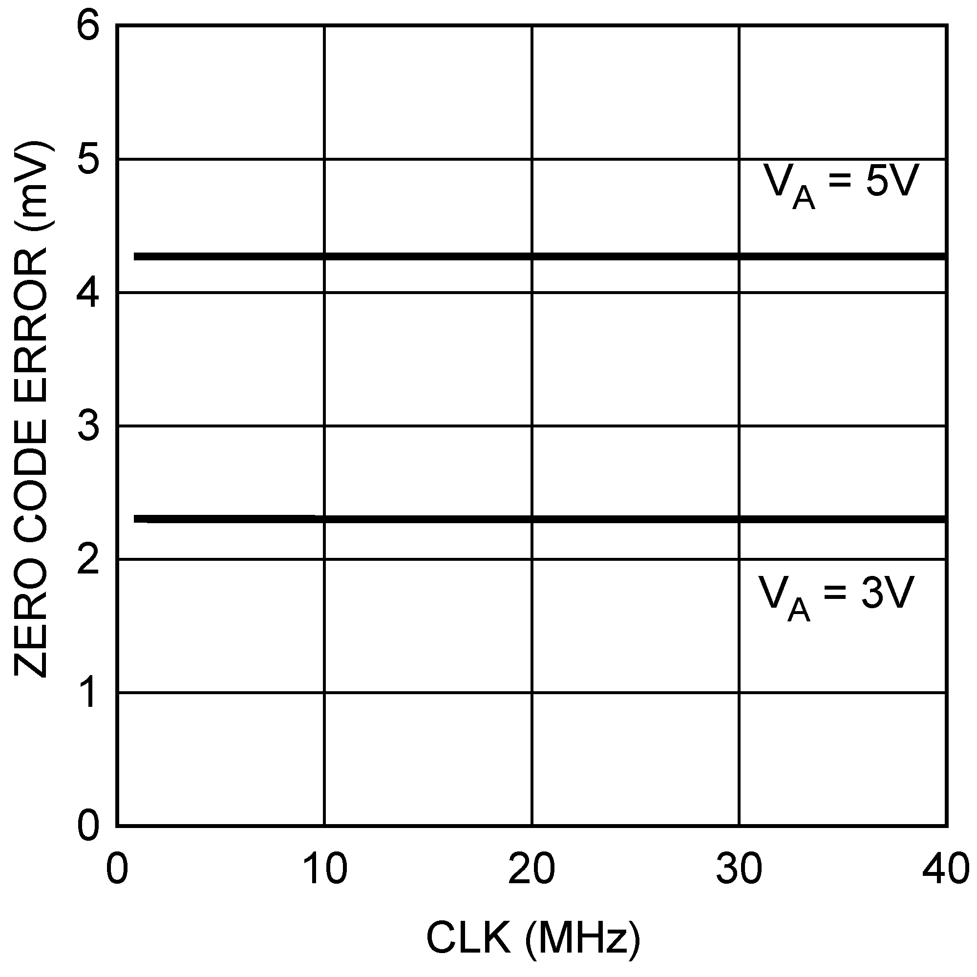
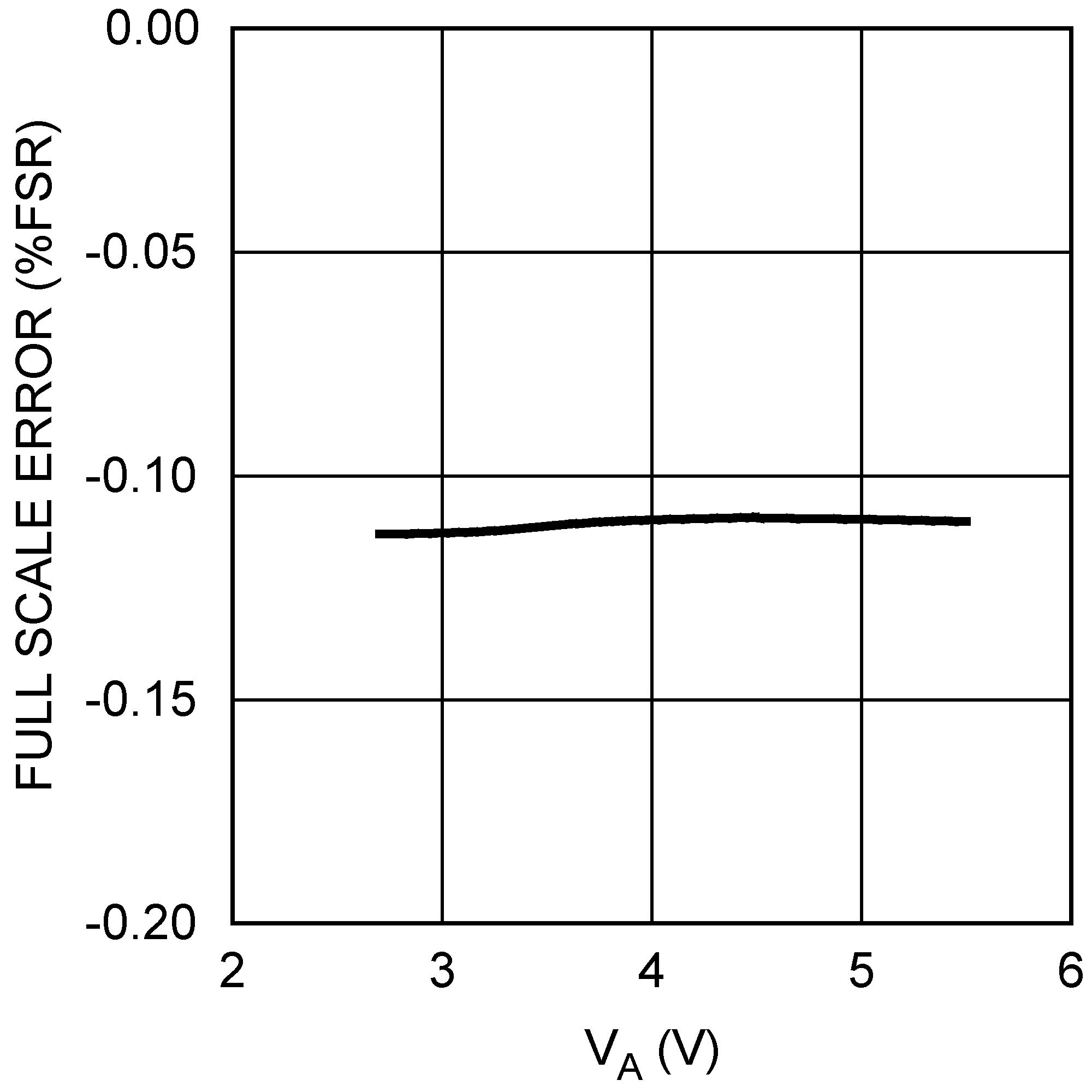
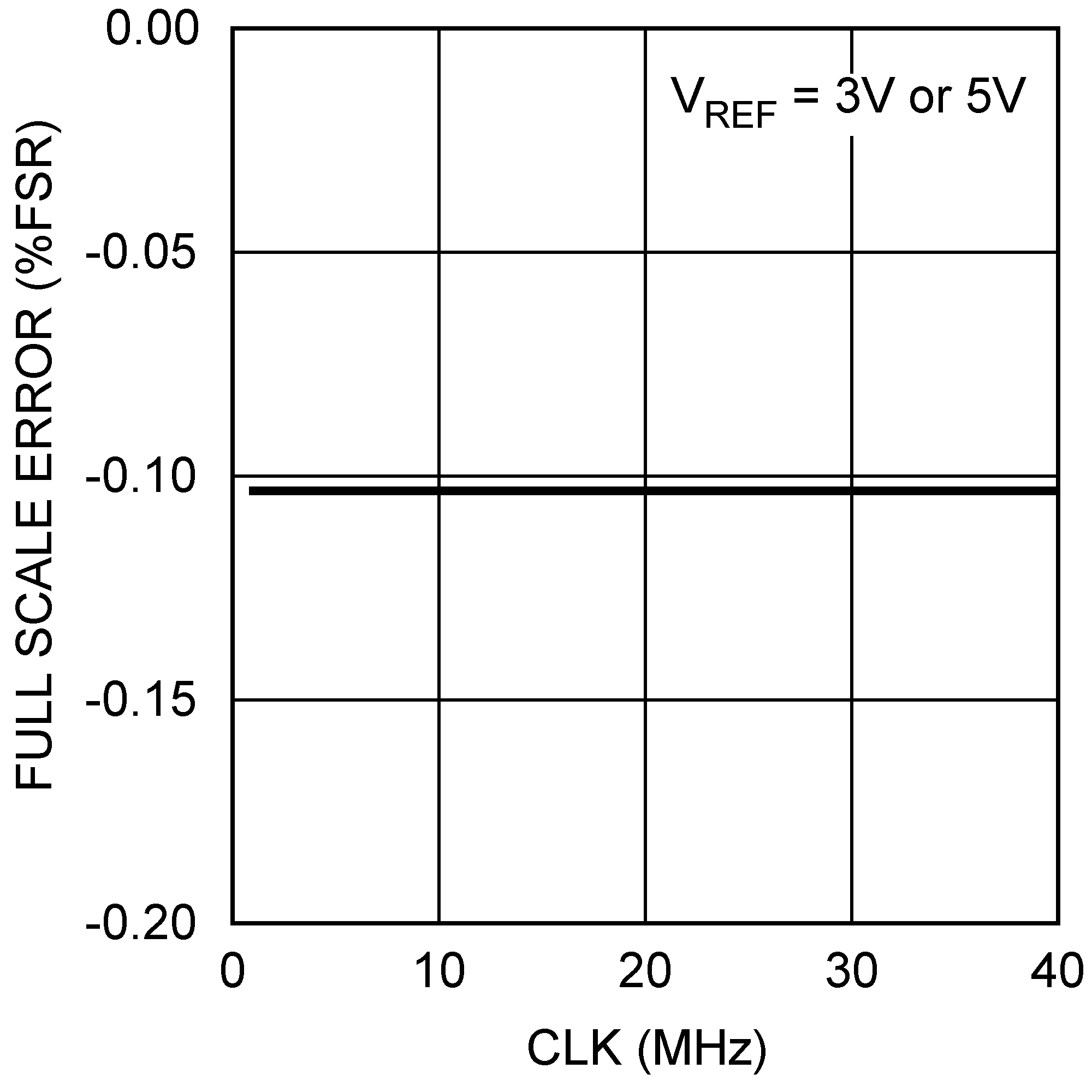
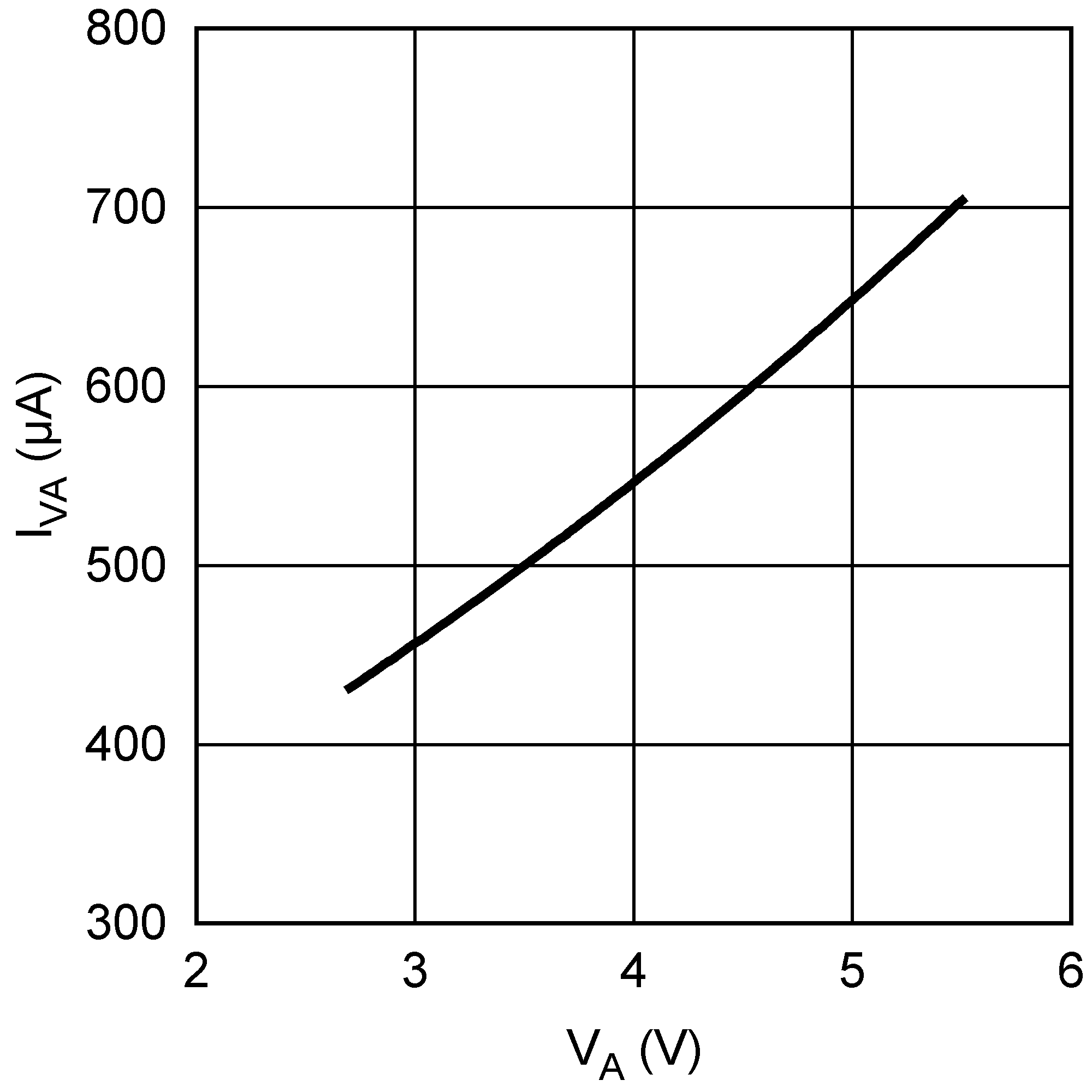
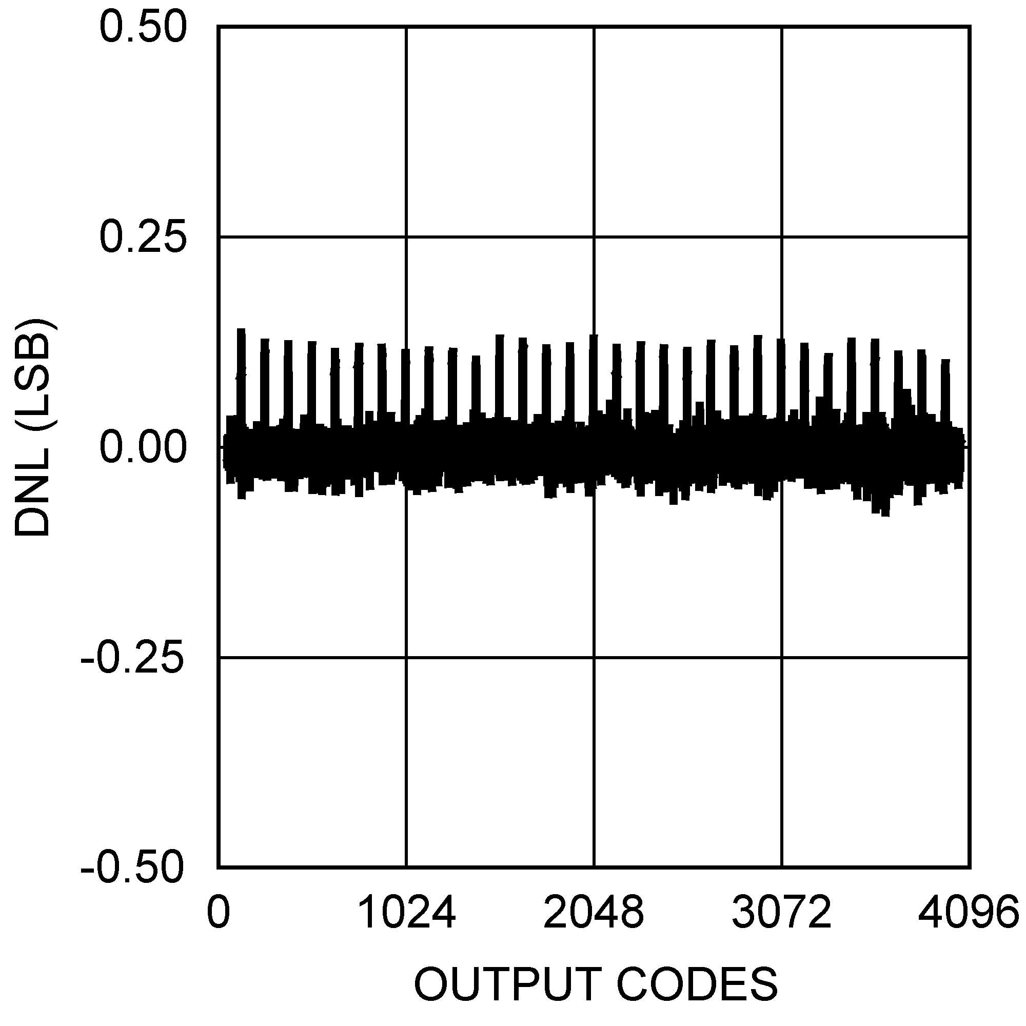
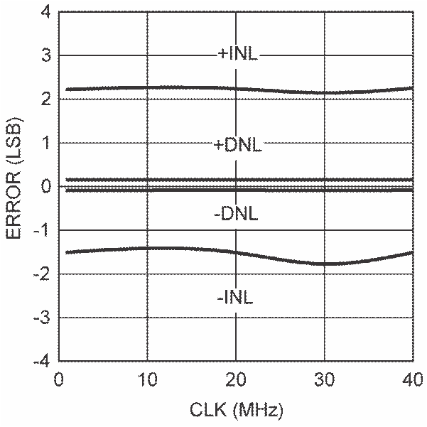
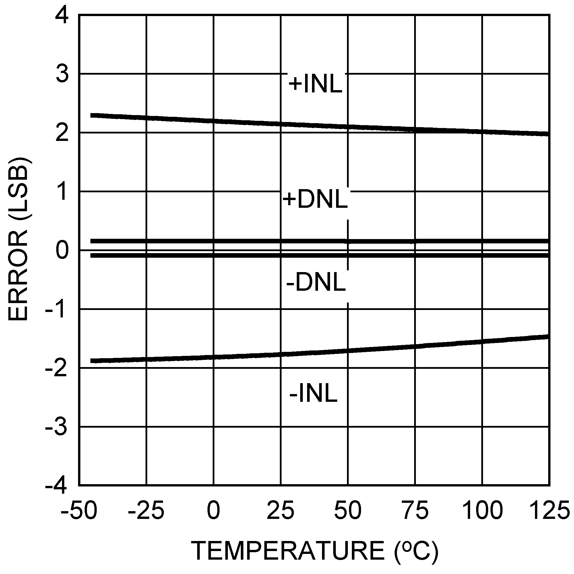
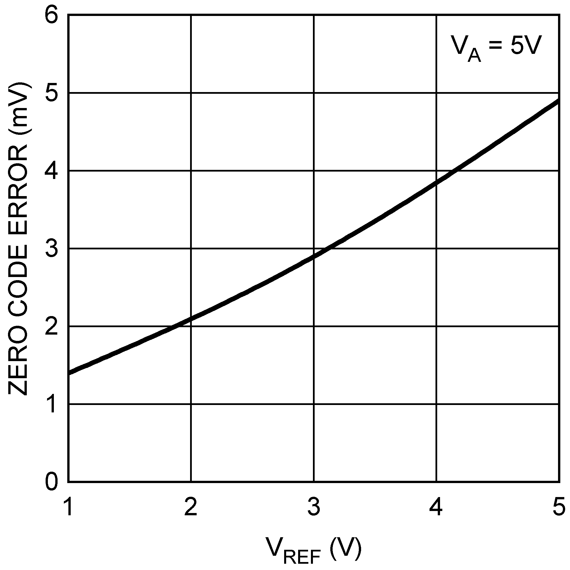
VA = 2.7 V to 5.5 V, VREF1,2 = VA, fSCLK = 30 MHz, TA = 25°C, unless otherwise stated