SNAA354A May 2021 – June 2022 ADC128S102QML-SP
4 Test Solution
To understand the sparkle behavior under multiple conditions a unique test solution had to be created to set the precise input conditions required to produce a sparkle code. The test solution has to be able to maintain the output code directly between the two codes listed under Code Transition in Table 3-1. During the test runs, data points before and after the detected sparkle code have to be collected. The test solution has to support collecting a significant number of conversions while monitoring the data for sparkle codes. The test solution also has to be robust, to repeat device behavior across different conditions.
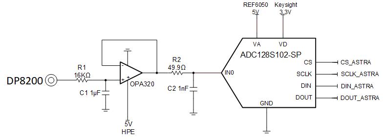
The hardware created had to support the half LSB accuracy requirement. To accomplish this the Data Precision Multifunction Calibrator (DP8200) was used. The equipment has a 10 ppm reading + 1 ppm range accuracy, has 1 uV resolution, and can be remotely controlled was used as the input signal source. To improve the noise performance a low pass filter consisting of a 16Kohm resister and 1uF capacitor was added with a cut off frequency of 10Hz. The input drive circuit consists of an OPA320 and a charge bucket filter (R2, C2) to drive the sample and hold capacitor shown in Figure 4-1. The ADC128S102-SP uses the analog power supply (VA) as the reference voltage to measure the output. VA is driven by the TI REF60xx family of precision voltage references., which have a total noise performance of 5uV_RMS. The reference, amplifier and digital power are provided by an external power supply, Keysight E363A or HPE3611A. The hardware was designed to use a socket to be able to change devices quickly and isolate the device for temperature measurements without exposing the surrounding circuitry using a thermal stream.
 Figure 4-1 Input Signal on Test Solution Schematic
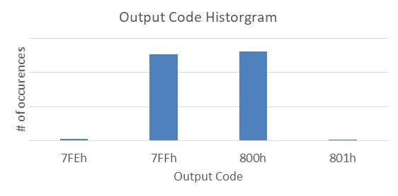
The ADC output is a digital representation of the analog input to ADC, thus to achieve a desired output code, the input voltage must be controlled to produce in the targeted output code. The algorithm used by the solution consist of a closed servo loop to control the input voltage based on the output code by controlling the DP8200 through GPIB cable, patent pending. The firmware can be thought of as two main functions, as shown in Figure 4-2, the Input Search Algorithm function and the Data Collection loop. The input search algorithm starts by bracketing the solution by a margin indicated by the user around the desired output code, and sets the input voltage to the midpoint of the bracket. The converter then completes 262,144 conversions and compares the average output code of this batch of conversions to the desired midpoint code transition. If the difference between the two values is not less than 0.1, then the input voltage is adjusted. To adjust the input, a half-interval search is used, if the error is greater than the desired value the upper bound is tightened by half and the same is done to the lower bound if the result is less than the desired value. The process continues as such until the average output code is within 0.1 codes of the midpoint code transition. This threshold is tighter than the targeted goal of half an LSB, which is the same as half a code. Referring to the previous example where the desired code and code-1 are 0x800 and 0x7FF, Figure 4-2 demonstrates an expected histogram of the output codes once the input algorithm is complete.
 Figure 4-2 Example Histogram of Output Code at Code Transition
Once the input produces the required output, the firmware enters the data collection loop. The data collection loop continuously converts data, in batches containing 262,144 conversions, and compares each output code within the batch to the expected sparkle code value. If a sparkle value is not present, then the average output is then compared to an extended error threshold of 0.12 LSB. This is to avoid the firmware jumping in and out of the loop too frequently; when collecting data at temperature extrema, this error threshold was increased to 0.35 LSB. In both cases this threshold is still within the half LSB requirement. If a sparkle is present, the batch containing the conversion results with the sparkle code is saved, this provides the outputs code before and after a sparkle code occurrence. From this point, the firmware continues on the same loop explained until the specified number of loops desired.
The firmware provides an accurate input voltage signal through the DP8200 and can account for drift within the system. Over time and temperature, the voltage reference, amplifier, and precision input source can drift. The average output code is checked against the error threshold before collecting a new batch of conversion results. If the average output code becomes greater than the error threshold (0.12 room temperature and 0.35 over temperature), then the firmware will return to the input search algorithm to re-adjusted the input voltage to force the output code into the proper range for sparkle detection.
The firmware is run on an in-house platform, ASTRA, which uses C based coding language, and drives the SPI bus to and from the converter.
 Figure 4-3 Test Solution Firmware Flow Map