SNAA354A May 2021 – June 2022 ADC128S102QML-SP
3 Root Cause Analysis
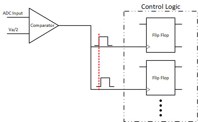
A multi-step ADC architecture, such as a successive approximation register (SAR) ADC, converts a continuous analog input voltage to a set of digital bits through a binary search. The binary search utilizes a high-speed decision loop to determine each bit value. The binary search starts by setting the most significant bit and comparing this value with the input voltage to determine the correct value and then setting the next significant bit. It repeats this decision loop, bit-by-bit, to build the remaining bits of the converted result. This process can introduce a sparkle code in the ADC128S102QML-SP due to the logic in the ADC having insufficient settling time. The design of the ADC128S102QML-SP is susceptible to sparkle codes due to the meta-stability of the bit-decision flip-flops used to determine the output conversion result.
A simplified block diagram is shown in Figure 3-1. The time margin for settling the flip-flops on the ADC128S102QML-SP decreased from the commercial version of the device due to the added circuitry required for radiation hardening. Note that these design differences make the ADC128S102QML-SP susceptible to sparkle codes, whereas the catalog version of the device is not susceptible to sparkle codes. It is also possible that sparkle code occurrence may be exacerbated at higher power supplies and lower temperatures as in these fast corner conditions there is less margin. Due to the nature of a sparkle code lot to lot variation cannot be bounded, and should be expected to vary as any other parametric would.
 Figure 3-1 Decision-Making Flip Flops Block Diagram
The source of a sparkle code occurrence is inherent to the digital circuitry of the ADC, and depends on the output code transition the ADC is measuring. A sparkle code may occur if the input voltage results in any lower subset of the digital code to toggle near a boundary where the most significant bit (MSB) of that subset is 0 and least significant bits (LSB) are all 1, or vice versa, where the most significant bit is 1 and the least significant bits are all 0. The output states described can be clearly seen in Table 3-1, which lists the ADC output code transitions and the respective possible sparkle value at that code transition. To further explain, a sparkle code is possible when the input voltage is at a binary multiple of the analog power supply, which acts as the reference voltage for this device. As an example, when the full-scale range is 5 V, the voltage step size is 1.2207 mV, which is equivalent to a least significant bit (LSB) and a single code increment. Therefore, an input voltage between 2.5 V and 2.49938 V (2.5 – 1 LSB) is now between the code transition 0×800 and 0×7FF. This will cause the ADC to naturally toggle between code and code ̶ 1 with equal probability based on quantization noise.
When the device is in this condition, a sparkle code is possible. Note that to achieve this condition, the input needs to have low noise and be equally within the code transition. If there is any noise, drift, or other sources of error, the output measurement could shift outside the code transition. If this occurs a sparkle code is no longer possible.
Each code transition will only sparkle to the respective listed sparkle value, no other value. The smallest sparkle delta as shown is 0×FF. The input voltage needs to be within half an LSB of this code transition for the device to output a sparkle code.
| Vin/Vref Ratio | Code Transition | Sparkle Code |
|---|---|---|
| 1/16 | 0×0FF - 0×100 | 0×1FF |
| 2/16 | 0×1FF - 0×200 | 0×3FF |
| 3/16 | 0×2FF - 0×300 | 0×200 |
| 4/16 | 0×3FF - 0×400 | 0×7FF |
| 5/16 | 0×4FF - 0×500 | 0×5FF |
| 6/16 | 0×5FF - 0×600 | 0×400 |
| 7/16 | 0×6FF - 0×700 | 0×600 |
| 8/16 | 0×7FF - 0×800 | 0×FFF |
| 9/16 | 0×8FF - 0×900 | 0×9FF |
| 10/16 | 0×9FF - 0×A00 | 0×BFF |
| 11/16 | 0×AFF - 0×B00 | 0×A00 |
| 12/16 | 0×BFF - 0×C00 | 0×800 |
| 13/16 | 0×CFF - 0×D00 | 0×DFF |
| 14/16 | 0×DFF - 0×E00 | 0×C00 |
| 15/16 | 0×EFF - 0×F00 | 0×E00 |