SLVUCA2 December 2021 TPS629210
3.7 Output Voltage Setting
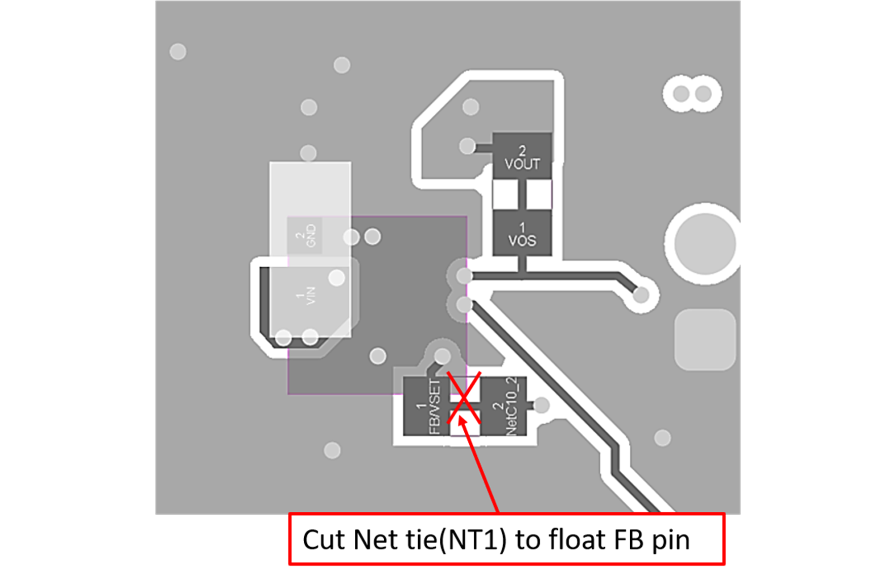
The TPS629210EVM is configured for external feedback as default with an output voltage of 3.3 V set by R1 and R2. Additionally, if the internal feedback (VSET) configuration is used, the user can cut net tie NT1 located on the back of the board. This modification is shown in Figure 3-1. This floats the FB pin, resulting in a 3.3-V output voltage using the internal VSET. Resistors R1 and R2 can also be changed to set the output voltage between 0.6 V and 5.5 V. See the TPS629210 3-V to 17-V, 1-A Low IQ Buck Converter in SOT583 Package data sheet for recommended values. R2 was populated with 34 k such that if the internal (VSET) is chosen while R1 is removed, the device regulates to 1.8-V output voltage.
 Figure 3-1 Internal Feedback (VSET) Configuration Board
Modification