SLVUC77 June 2021 DRV8770
2 PCB Connectors and Headers
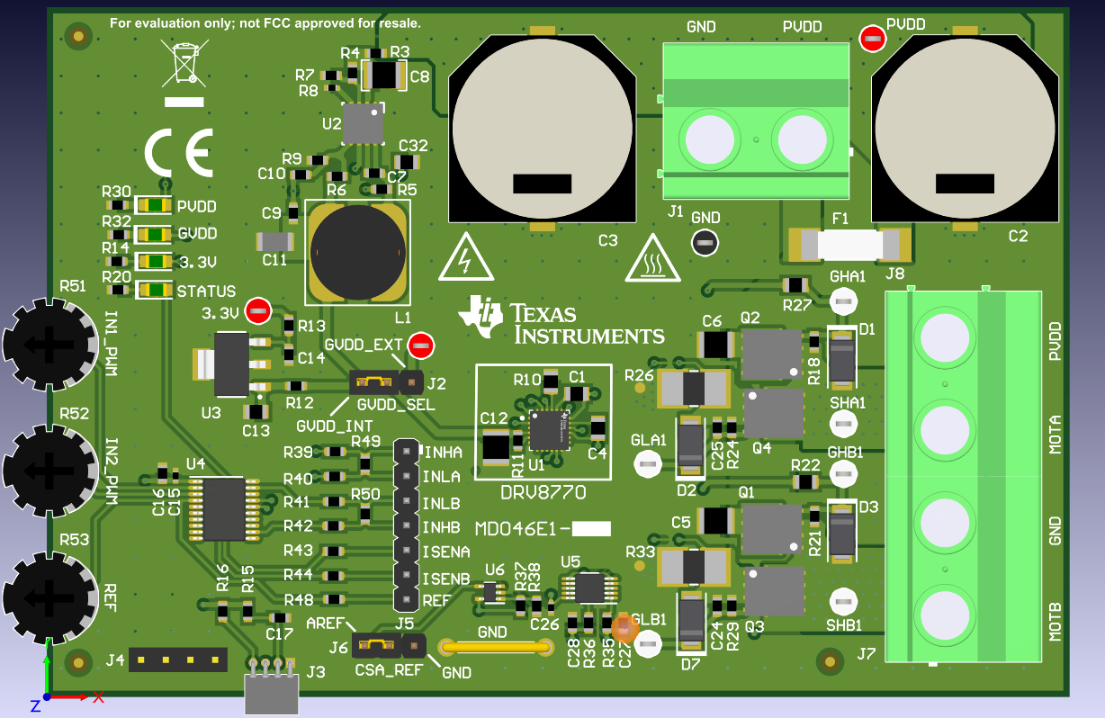
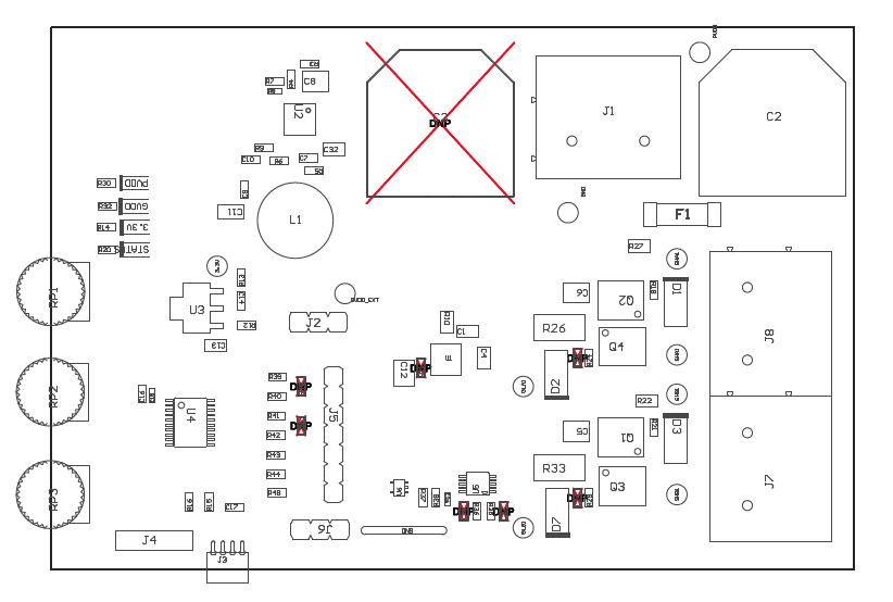
The DRV8770EVM top PCB view and top assembly view are shown in Figure 2-2 and Figure 2-1. The board connectors and headers are listed and described in Table 2-1.

Figure 2-1 DRV8770EVM PCB Top View
 Figure 2-2 DRV8770EVM Top Assembly
View
Figure 2-2 DRV8770EVM Top Assembly
ViewTable 2-1 Board Component and Connector
| Component | Function |
|---|---|
| J1 | PVDD supply connector |
| J7/J8 | Output connector (MOTA, MOTB, PVDD, GND) |
| J2 | Header for GVDD supply selection. If shorted between middle pin and "GVDD_INT" pin, GVDD will come from internal buck converter. If middle pin and "GVDD_EXT" is shorted, GVDD supply will come from external source connected to "GVDD_EXT" red test point. |
| J3 | Connector for programming the MCU on the board. |
| J4 | Header connected to J3 connector. Can manually place jumper wires to Spi-By-Wire pins on the LaunchPad |
| J5 | Main control signal header test poin. |
| J6 | Current sense amplifier (CSA) reference voltage selector header. Short middle pin to "AREF" to set REF voltage of CSA to 1.65-V (mainly used for bi-directional current sensing). Short middle pin to "GND" to set the CSA REF voltage to 0-V. |
| PVDD LED | PVDD LED indication |
| GVDD LED | GVDD LED indication |
| 3.3 V LED | 3.3 V LED indication |
| STATUS LED | MCU STATUS LED indicator. Will turn ON when MCU is working |
| RP1 | Potentiometer for adjusting duty cycle of INHA and INLA |
| RP2 | Potentiometer for adjusting duty cycle of INHB and INLB |
| RP3 | Unused potentiometer. |